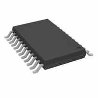
AD5206BRU100 Analog Devices Inc, AD5206BRU100 Datasheet - Page 15

AD5206BRU100
Manufacturer Part Number
AD5206BRU100
Description
IC,Digital Potentiometer,CMOS,TSSOP,24PIN,PLASTIC
Manufacturer
Analog Devices Inc
Datasheet
1.AD5204BRUZ50.pdf
(20 pages)
Specifications of AD5206BRU100
Rohs Status
RoHS non-compliant
Taps
256
Resistance (ohms)
100K
Number Of Circuits
6
Temperature Coefficient
700 ppm/°C Typical
Memory Type
Volatile
Interface
SPI, 3-Wire Serial
Voltage - Supply
2.7 V ~ 5.5 V, ±2.3 V ~ 2.7 V
Operating Temperature
-40°C ~ 85°C
Mounting Type
Surface Mount
Package / Case
24-TSSOP
Resistance In Ohms
100K
Lead Free Status / RoHS Status
DIGITAL INTERFACING
The AD5204/AD5206 each contain a standard 3-wire serial
input control interface. The three inputs are clock (CLK), chip
select input ( CS ), and serial data input (SDI). The positive-
edge-sensitive CLK input requires clean transitions to avoid
clocking incorrect data into the serial input register. Standard
logic families work well. If mechanical switches are used for
product evaluation, they should be debounced by a flip-flop or
by other suitable means.
internal digital circuitry. When
loads data into the serial register on each positive clock edge
(see
supply voltage, the logic levels are still referenced to digital
ground (GND).
The serial data output (SDO) pin contains an open-drain
n-channel FET. This output requires a pull-up resistor to transfer
data to the SDI pin of the next package. The pull-up resistor
termination voltage can be larger than the V
AD5204. For example, the AD5204 can operate at V
and the pull-up for the interface to the next device can be set at
5 V. This allows for daisy chaining several RDACs from a
single-processor serial data line.
If a pull-up resistor is used to connect the SDI pin of the
next device in the series, the clock period must be increased.
Capacitive loading at the daisy-chain node (where SDO and
SDI are connected) between the devices must be accounted for
to successfully transfer data. When daisy chaining is used, the
CS should be kept low until all the bits of every package are
clocked into their respective serial registers, ensuring that the
address bits and data bits are in the proper decoding locations.
This requires 22 bits of address and data complying to the data-
word format outlined in
are daisy-chained. During shutdown (
pin is forced to the off (logic high state) position to disable power
dissipation in the pull-up resistor. See
SDO output circuit schematic.
Table 9. Input Logic Control Truth Table
CLK
L
P
X
X
X
X
X
1
P = positive edge, X = don’t care, SR = shift register.
Table 9
CS
L
L
P
H
X
H
H
). When using a positive (V
PR
H
H
H
H
L
P
H
SHDN
H
H
H
H
H
H
L
Table 6
Figure 22
No SR effect; enables SDO pin.
No operation.
Latches all RDAC latches to 0x80.
Register Activity
Shift one bit in from the SDI pin. The
11
SDO pin.
Load SR data into the RDAC latch
based on A2, A1, A0 decode (Table 10).
Sets all RDAC latches to midscale;
wiper centered and SDO latch
cleared.
Open circuits all A resistor terminals,
connects Wiper W to Terminal B, and
turns off the SDO output transistor.
th
if two AD5204 4-channel RDACs
bit entered is shifted out of the
CS is taken active low, the clock
shows more detail of the
Figure 24
SHDN ), the SDO output
DD
) and negative (V
1
DD
for the equivalent
supply of the
DD
= 3.3 V,
SS
)
Rev. C | Page 15 of 20
Table 10. Address Decode Table
A2
0
0
0
0
1
1
The data setup and data hold times in the specification table
determine the data valid time requirements. The last 11 bits of
the data-word entered into the serial register are held when CS
returns high. When CS goes high, the address decoder is gated,
enabling one of four or six positive-edge-triggered RDAC
latches (see
The target RDAC latch is loaded with the last eight bits of the
serial data-word, completing one DAC update. Four separate
8-bit data-words must be clocked in to change all four VR
settings.
All digital pins ( CS , SDI, SDO, PR , SHDN , and CLK) are
protected with a series input resistor and a parallel Zener ESD
structure (see
SHDN
A1
0
0
1
1
0
0
Figure 24. Detail SDO Output Schematic of the AD5204
CLK
SDI
CLK
CS
PR
SDI
CS
Figure 23
AD5204/AD5206
Figure 25
Figure 23. Equivalent Input Control Logic
REGISTER
SERIAL
A0
0
1
0
1
0
1
for details).
).
D
CK RS
Latch Decoded
RDAC 1
RDAC 2
RDAC 3
RDAC 4
RDAC 5 AD5206 only
RDAC 6 AD5206 only
Q
DECODE
REGISTER
ADDR
SERIAL
AD5204/AD5206
RDAC 1
RDAC 2
RDAC 4/
RDAC 6
SDO
GND


