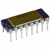
AD539KDZ Analog Devices Inc, AD539KDZ Datasheet

AD539KDZ
Specifications of AD539KDZ
Related parts for AD539KDZ
AD539KDZ Summary of contents
Page 1
FEATURES 2-quadrant multiplication/division 2 independent signal channels Signal bandwidth of 60 MHz (I ) OUT Linear control channel bandwidth of 5 MHz Low distortion (to 0.01%) Fully calibrated, monolithic circuit APPLICATIONS Precise high bandwidth AGC and VCA systems Voltage-controlled filters ...
Page 2
AD539 TABLE OF CONTENTS Features .............................................................................................. 1 Applications....................................................................................... 1 Functional Block Diagram .............................................................. 1 General Description ......................................................................... 1 Revision History ............................................................................... 2 Specifications..................................................................................... 3 Pin Configurations and Function Descriptions ........................... 5 Typical Performance Characteristics ............................................. 7 Theory of Operation ...................................................................... ...
Page 3
SPECIFICATIONS T = 25° ±5 V, unless otherwise specified guaranteed. Table 1. Parameter Test Conditions/Comments SIGNAL CHANNEL DYNAMICS See Figure 22 Minimal Configuration Bandwidth, − Ω Maximum Output 0.1 ...
Page 4
AD539 Parameter Test Conditions/Comments CONTROL INPUT Nominal Full-Scale Input Operational Range, Degraded Performance 2 Input Resistance Offset Voltage MIN MAX Power Supply Sensitivity See Figure 20 Gain Absolute Gain Error ...
Page 5
PIN CONFIGURATIONS AND FUNCTION DESCRIPTIONS Table 2. 20-Lead LLC Pin Function Descriptions Pin No. Mnemonic COMP – INPUT COMMON ...
Page 6
AD539 Table 3. 16-Lead PDIP and SBDIP Pin Function Descriptions Pin No. Mnemonic COMP – INPUT COMMON 8 OUTPUT COMMON ...
Page 7
TYPICAL PERFORMANCE CHARACTERISTICS − – unless otherwise noted AD539K 0 SPECS –1 –2 –3 0.01 0.1 CONTROL VOLTAGE (V Figure 4. ...
Page 8
AD539 –1 – FREQUENCY (MHz) Figure 10. Phase Linearity Error in Minimal Configuration 5 0. –2.5 –5.0 –2 ...
Page 9
Figure 16. Transient Response of the Voltage-Controlled Amplifier ± +0.01V +0.032V +0. ...
Page 10
AD539 THEORY OF OPERATION CIRCUIT DESCRIPTION Figure 18 shows a simplified schematic of the AD539 are large-geometry transistors designed for low distortion and low noise. Emitter-area scaling further reduces distortion three times larger than Q2; ...
Page 11
The power supplies to the AD539 can be as low as ±4.5 V and as high as ±16.5 V. The maximum allowable range of the signal inputs approximately 0.5 V above +V Y value is 2.5 V ...
Page 12
AD539 APPLICATIONS INFORMATION BASIC MULTIPLIER CONNECTIONS Figure 20 shows the connections for the standard dual-channel multiplier, using op amps to provide useful output power and the AD539 feedback resistors to achieve accurate scaling. The transfer function for each channel is ...
Page 13
Table 4. Summary of Operating Conditions and Performance for the AD539 When Used with Various External Op Amp Output Amplifiers Operating Conditions AD711 Op Amp Supply Voltages ± Amp Compensation Capacitor None Feedback Capacitor, C None F −3 ...
Page 14
AD539 Differential Configurations When only one signal channel must be handled often advantageous to use the channels differentially. By subtracting the Channel 1 and Channel 2 outputs, any residual transient control feedthrough is virtually eliminated. Figure 22 shows ...
Page 15
A 50 MHZ VOLTAGE-CONTROLLED AMPLIFIER Figure circuit for a 50 MHz voltage-controlled amplifier (VCA) suitable for use in high quality video-speed applications. The outputs from the two signal channels of the AD539 are applied to the op ...
Page 16
AD539 BASIC DIVIDER CONNECTIONS Standard Scaling The AD539 provides excellent operation as a two-quadrant analog divider in wideband, wide gain-range applications, with the advantage of dual-channel operation. Figure 25 shows the simplest connections for division with a transfer function of ...
Page 17
OUTLINE DIMENSIONS 0.210 (5.33) MAX 0.150 (3.81) 0.130 (3.30) 0.115 (2.92) 0.022 (0.56) 0.018 (0.46) 0.014 (0.36) CONTROLLING DIMENSIONS ARE IN INCHES; MILLIMETER DIMENSIONS (IN PARENTHESES) ARE ROUNDED-OFF INCH EQUIVALENTS FOR REFERENCE ONLY AND ARE NOT APPROPRIATE FOR USE IN ...
Page 18
... PARENTHESES) ARE ROUNDED-OFF INCH EQUIVALENTS FOR REFERENCE ONLY AND ARE NOT APPROPRIATE FOR USE IN DESIGN. ORDERING GUIDE 1 Model Notes AD539JN AD539JNZ AD539JDZ AD539KN AD539KNZ AD539KDZ AD539SD AD539SD/883B 2 5962-8980901EA AD539SE/883B RoHS Compliant Part. 2 The standard military drawing version of the AD539 (5962-8980901EA) is now available. 0.075 (1.91) REF 0 ...
Page 19
NOTES Rev Page AD539 ...
Page 20
AD539 NOTES ©1983–2011 Analog Devices, Inc. All rights reserved. Trademarks and registered trademarks are the property of their respective owners. D09679-0-4/11(B) Rev Page ...


