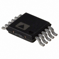
AD5426YRM Analog Devices Inc, AD5426YRM Datasheet - Page 22

AD5426YRM
Manufacturer Part Number
AD5426YRM
Description
8-IOUT DAC WITH SERIAL ITF I.C.
Manufacturer
Analog Devices Inc
Datasheet
1.AD5443YRMZ.pdf
(28 pages)
Specifications of AD5426YRM
Rohs Compliant
NO
Rohs Status
RoHS non-compliant
Design Resources
Unipolar, Precision DC Digital-to-Analog Conversion Using AD5426/32/43 8-Bit to12-Bit DACs (CN0034) Precision, Bipolar Configuration for the AD5426/32/43 8-Bit to12-Bit DACs (CN0036) AC Signal Processing Using AD5426/32/43 Current Output DACs (CN0037) Programmable Gain Element Using AD5426/32/43 Current Output DACs (CN0038)
Number Of Bits
8
Data Interface
Serial
Number Of Converters
1
Voltage Supply Source
Single Supply
Operating Temperature
-40°C ~ 125°C
Mounting Type
Surface Mount
Package / Case
10-MSOP, Micro10™, 10-uMAX, 10-uSOP
Power Dissipation (max)
25µW
Settling Time
50ns
Lead Free Status / RoHS Status
Available stocks
Company
Part Number
Manufacturer
Quantity
Price
Part Number:
AD5426YRM
Manufacturer:
ADI/亚德诺
Quantity:
20 000
Company:
Part Number:
AD5426YRMZ
Manufacturer:
MAX
Quantity:
26
Part Number:
AD5426YRMZ
Manufacturer:
ADI/亚德诺
Quantity:
20 000
AD5426/AD5432/AD5443
80C51/80L51 to AD5426/AD5432/AD5443 Interface
A serial interface between the DAC and the 8051 is shown in
Figure 55. TxD of the 8051 drives SCLK of the DAC serial
interface, while RxD drives the serial data line, D
programmable pin on the serial port and is used to drive SYNC .
When data is to be transmitted to the switch, P3.3 is taken low.
The 80C51/80L51 transmits data only in 8-bit bytes; thus, only
eight falling clock edges occur in the transmit cycle. To load
data correctly to the DAC, P3.3 is left low after the first eight
bits are transmitted, and a second write cycle is initiated to
transmit the second byte of data. Data on RxD is clocked out of
the microcontroller on the rising edge of TxD and is valid on
the falling edge. As a result, no glue logic is required between
the DAC and microcontroller interface. P3.3 is taken high
following the completion of this cycle. The 8051 provides the
LSB of its SBUF register as the first bit in the data stream. The
DAC input register requires its data with the MSB as the first bit
received. The transmit routine should take this into account.
MC68HC11 Interface to AD5426/AD5432/AD5443
Interface
Figure 56 shows an example of a serial interface between the
DAC and the MC68HC11 microcontroller. The SPI on the
MC68HC11 is configured for master mode (MSTR) = 1, clock
polarity bit (CPOL) = 0, and the clock phase bit (CPHA) = 1.
The SPI is configured by writing to the SPI control register
(SPCR)—see the 68HC11 user manual. SCK of the 68HC11
drives the SCLK of the DAC interface, the MOSI output drives
the serial data line (DIN) of the AD5426/AD5432/AD5443. The
SYNC signal is derived from a port line (PC7). When data is
being transmitted to the DAC, the SYNC line is taken low
(PC7). Data appearing on the MOSI output is valid on the
falling edge of SCK. Serial data from the 68HC11 is transmitted
in 8-bit bytes with only eight falling clock edges occurring in
the transmit cycle. Data is transmitted MSB first. To load data
to the DAC, PC7 is left low after the first eight bits are
transferred and a second serial write operation is performed to
the DAC. PC7 is taken high at the end of this procedure.
If the user wants to verify the data previously written to the
input shift register, the SDO line can be connected to MISO of
the MC68HC11, and with SYNC low, the shift register would
clock data out on the rising edges of SCLK.
ADDITIONAL PINS OMITTED FOR CLARITY.
Figure 55. 80C51/80L51-to-AD5426/AD5432/AD5443 Interface
8051
RxD
P1.1
TxD
SCLK
SDIN
SYNC
IN
AD5426/
AD5432/
AD5443
. P3.3 is a bit-
Rev. C | Page 22 of 28
MICROWIRE to AD5426/AD5432/AD5443 Interface
Figure 57 shows an interface between the DAC and any
MICROWIRE-compatible device. Serial data is shifted out on
the falling edge of the serial clock, SK, and is clocked into the
DAC input shift register on the rising edge of SK, which
corresponds to the falling edge of the DACs SCLK.
PIC16C6x/7x to AD5426/AD5432/AD5443
The PIC16C6x/7x synchronous serial port (SSP) is configured
as an SPI master with the clock polarity bit (CKP) = 0. This is
done by writing to the synchronous serial port control register
(SSPCON). See the PIC16/17 Microcontroller User Manual. In
this example, I/O port RA1 is being used to provide a SYNC
signal and to enable the serial port of the DAC. This
microcontroller transfers only eight bits of data during each
serial transfer operation; therefore, two consecutive write
operations are required.
diagram.
ADDITIONAL PINS OMITTED FOR CLARITY.
ADDITIONAL PINS OMITTED FOR CLARITY.
ADDITIONAL PINS OMITTED FOR CLARITY.
MICROWIRE
PIC16C6x/7x
Figure 56. 68HC11/68L11-to-AD5426/AD5432/AD5443 Interface
MC68HC11
Figure 58. PIC16C6x/7x-to-AD5426/AD5432/AD5443 Interface
Figure 57. MICROWIRE-to-AD5426/AD5432/AD5443 Interface
SCK/RC3
SDI/RC4
MOSI
SCK
RA1
PC7
SK
SO
CS
Figure 58
shows the connection
SYNC
SCLK
SDIN
SCLK
SDIN
SYNC
SCLK
SDIN
SYNC
AD5426/
AD5432/
AD5443
AD5426/
AD5432/
AD5443
AD5426/
AD5432/
AD5443


