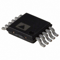
AD5432YRM Analog Devices Inc, AD5432YRM Datasheet - Page 16

AD5432YRM
Manufacturer Part Number
AD5432YRM
Description
10-IOUT DAC WITH SERIAL ITF I.C.
Manufacturer
Analog Devices Inc
Datasheet
1.AD5443YRMZ.pdf
(28 pages)
Specifications of AD5432YRM
Rohs Compliant
NO
Rohs Status
RoHS non-compliant
Design Resources
Unipolar, Precision DC Digital-to-Analog Conversion Using AD5426/32/43 8-Bit to12-Bit DACs (CN0034) Precision, Bipolar Configuration for the AD5426/32/43 8-Bit to12-Bit DACs (CN0036) AC Signal Processing Using AD5426/32/43 Current Output DACs (CN0037) Programmable Gain Element Using AD5426/32/43 Current Output DACs (CN0038)
Number Of Bits
10
Data Interface
Serial
Number Of Converters
1
Voltage Supply Source
Single Supply
Operating Temperature
-40°C ~ 125°C
Mounting Type
Surface Mount
Package / Case
10-MSOP, Micro10™, 10-uMAX, 10-uSOP
Power Dissipation (max)
25µW
Settling Time
50ns
Lead Free Status / RoHS Status
Available stocks
Company
Part Number
Manufacturer
Quantity
Price
Part Number:
AD5432YRM
Manufacturer:
ADI/亚德诺
Quantity:
20 000
Part Number:
AD5432YRMZ
Manufacturer:
ADI/亚德诺
Quantity:
20 000
Part Number:
AD5432YRMZ-REEL7
Manufacturer:
ADI/亚德诺
Quantity:
20 000
AD5426/AD5432/AD5443
Bipolar Operation
In some applications, it may be necessary to generate full
4-quadrant multiplying operation or a bipolar output swing.
This can easily be accomplished by using another external
amplifier and some external resistors, as shown in Figure 42. In
this circuit, the second amplifier, A2, provides a gain of 2.
Biasing the external amplifier with an offset from the reference
voltage results in full 4-quadrant multiplying operation. The
transfer function of this circuit shows that both negative and
positive output voltages are created as the input data, D, which
is incremented from code zero (V
(V
where D is the fractional representation of the digital word
loaded to the DAC and n is the resolution of the DAC.
When V
multiplication.
Table 6 shows the relationship between digital code and the
expected output voltage for bipolar operation (AD5426,
8-bit device).
OUT
D= 0 to 255 (8-bit AD5426)
V
= 0 V) to full scale (V
OUT
= 0 to 1023 (10-bit AD5432)
= 0 to 4095 (12-bit AD5443)
IN
is an ac signal, the circuit performs 4-quadrant
=
⎛
⎜
⎝
V
REF
×
2
n
D
− 1
⎞
⎟
⎠
OUT
−
V
V
±10V
REF
= +V
REF
OUT
NOTES
1. R1 AND R2 ARE USED ONLY IF GAIN ADJUSTMENT IS REQUIRED. ADJUST R1 FOR
2. MATCHING AND TRACKING IS ESSENTIAL FOR RESISTOR PAIRS R3 AND R4.
3. C1 PHASE COMPENSATION (1pF TO 2pF) MAY BE REQUIRED IF A1/A2 IS A HIGH
V
SPEED AMPLIFIER.
REF
OUT
= −V
R1
).
= 0V WITH CODE 10000000 LOADED TO DAC.
REF
MICROCONTROLLER
SYNC
V
) to midscale
REF
SCLK SDIN GND
AD5426/
AD5432/
AD5443
V
V
DD
DD
Figure 42. Bipolar Operation
R
FB
Rev. C | Page 16 of 28
20kΩ
I
I
OUT
OUT
R3
1
2
R2
C1
AGND
Table 6. Bipolar Code Table
Digital Input
1111 1111
1000 0000
0000 0001
0000 0000
Stability
In the I-to-V configuration, the I
inverting node of the op amp must be connected as close as
possible and proper PCB layout techniques must be employed.
Since every code change corresponds to a step function, gain
peaking may occur if the op amp has limited gain bandwidth
product (GBP) and there is excessive parasitic capacitance at the
inverting node. This parasitic capacitance introduces a pole into
the open-loop response that can cause ringing or instability in
closed-loop applications.
An optional compensation capacitor, C1, can be added in
parallel with R
Too small a value of C1 can produce ringing at the output, while
too large a value can adversely affect the settling time. C1 should be
found empirically, but 1 pF to 2 pF is generally adequate for
compensation.
A1
A1
10kΩ
R4
FB
for stability, as shown in Figure 41 and Figure 42.
20kΩ
A2
R5
V
TO +V
OUT
= –V
REF
REF
Analog Output (V)
+V
0
−V
−V
REF
REF
REF
OUT
(127/128)
(127/128)
(128/128)
of the DAC and the


