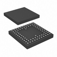
AD5532ABC-1 Analog Devices Inc, AD5532ABC-1 Datasheet - Page 15

AD5532ABC-1
Manufacturer Part Number
AD5532ABC-1
Description
D/A Converter (D-A) IC
Manufacturer
Analog Devices Inc
Datasheet
1.AD5532ABCZ-1.pdf
(20 pages)
Specifications of AD5532ABC-1
No. Of Bits
14 Bit
No. Of Channels
32
No. Of Outputs
8
Rohs Status
RoHS non-compliant
Settling Time
22µs
Number Of Bits
14
Data Interface
Serial
Number Of Converters
34
Voltage Supply Source
Analog and Digital
Power Dissipation (max)
623mW
Operating Temperature
-40°C ~ 85°C
Mounting Type
Surface Mount
Package / Case
74-CSPBGA
For Use With
EVAL-AD5532HSEBZ - BOARD EVAL FOR AD5532HSEVAL-AD5532EBZ - BOARD EVAL FOR AD5532
Lead Free Status / RoHS Status
Available stocks
Company
Part Number
Manufacturer
Quantity
Price
Company:
Part Number:
AD5532ABC-1
Manufacturer:
ADI
Quantity:
150
Company:
Part Number:
AD5532ABC-1
Manufacturer:
Analog Devices Inc
Quantity:
10 000
TRACK FUNCTION (ISHA MODE)
Typically in ISHA mode of operation TRACK is held high and
the channel begins to acquire when it is addressed. However, if
TRACK is low when the channel is addressed, V
the output buffer and an acquisition on the channel does not
occur until a rising edge of TRACK . At this stage, the BUSY pin
goes low until the acquisition is complete, at which point the
DAC assumes control of the voltage to the output buffer and V
is free to change again without affecting this output value.
This is useful in an application where the user wants to ramp up
V
does not need to be acquired continuously while it is ramping
up. TRACK can be kept low and only when V
desired voltage is TRACK brought high. At this stage, the
acquisition of V
In the example shown, a desired voltage is required on the
output of the pin driver. This voltage is represented by one input
to a comparator. The microcontroller/microprocessor ramps up
the input voltage on V
while the voltage on V
acquired. When the desired voltage is reached on the output of
the pin driver, the comparator output switches. The μC/μP then
knows what code is required to be input to obtain the desired
voltage at the DUT. The TRACK input is now brought high and
the part begins to acquire V
V
V
MODES OF OPERATION
The AD5532 can be used in four different modes of operation.
These modes are set by two mode bits, the first two bits in the
serial word.
Table 9. Modes of Operation
Mode Bit 1
0
0
1
1
IN
IN
IN
until V
has been acquired. The output buffer is then switched from
to the output of the DAC.
OUT
reaches a particular level (see Figure 20). V
IN
Mode Bit 2
0
1
0
1
begins.
CONTROLLER
IN
IN
through a DAC. TRACK is kept low
ramps up so that V
IN
. At this stage BUSY goes low until
Operating Mode
ISHA mode
DAC mode
Acquire and Read Back
Read Back
DAC
TRACK
BUSY
IN
V
OUT
is not continually
IN
IN
ONLY ONE CHANNEL SHOWN FOR SIMPLICITY
has reached its
Figure 20. Typical ATE Circuit Using TRACK Input
is switched to
ACQUISITION
CIRCUIT
IN
Rev. D | Page 15 of 20
IN
1. ISHA Mode
In this mode, a channel is addressed and that channel acquires
the voltage on V
21a) to address the relevant channel (V
channel or all channels). MSB is written first.
2. DAC Mode
In this standard mode, a selected DAC register is loaded serially.
This requires a 24-bit write (10 bits to address the relevant DAC
plus an extra 14 bits of DAC data). MSB is written first. The
user must allow 400 ns (min) between successive writes in DAC
mode.
3. Acquire and Readback Mode
This mode allows the user to acquire V
in a particular DAC register. The relevant channel is addressed
(10-bit write, MSB first) and V
Following the acquisition, after the next falling edge of SYNC ,
the data in the relevant DAC register is clocked out onto the
D
must elapse before the DAC register data can be clocked out.
4. Readback Mode
Again, this is a Readback mode but no acquisition is performed.
The relevant channel is addressed (10-bit write, MSB first) and
on the next falling edge of SYNC , the data in the relevant DAC
register is clocked out onto the D
format. The user must allow 400 ns (min) between the last
SCLK falling edge in the 10-bit write and the falling edge of
SYNC in the 14-bit read back. The serial write and read words
can be seen in
This feature allows the user to read back the DAC register code
of any of the channels. In DAC mode, this is useful in
verification of write cycles. In ISHA mode, readback is useful if
the system has been calibrated and the user wants to know what
code in the DAC corresponds to a desired voltage on V
this voltage is required again, the user can input the code
directly to the DAC register without going through the
acquisition sequence.
AD5532
OUTPUT
STAGE
OUT
line in a 14-bit serial format. The full acquisition time
V
OUT
Figure 21
IN
1
. This mode requires a 10-bit write (see Figure
DRIVER
THRESHOLD
VOLTAGE
PIN
.
IN
is acquired in 16 μs (max).
OUT
line in a 14-bit serial
OUT
IN
and read back the data
DEVICE
UNDER
TEST
0–V
OUT
31, offset
AD5532
OUT
. If


