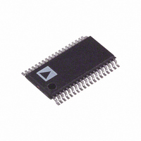
AD5557CRU Analog Devices Inc, AD5557CRU Datasheet - Page 6

AD5557CRU
Manufacturer Part Number
AD5557CRU
Description
IC,D/A CONVERTER,DUAL,14-BIT,TSSOP,38PIN
Manufacturer
Analog Devices Inc
Datasheet
1.AD5547BRUZ.pdf
(20 pages)
Specifications of AD5557CRU
Design Resources
Precision, Unipolar, Inverting Conversion Using AD5547/57 DAC (CN0026) Precision, Unipolar, Noninverting Configuration for the AD5547/57 DAC (CN0027) Precision, Bipolar, Configuration for AD5547/AD5557 DAC (CN0028)
Settling Time
500ns
Number Of Bits
14
Data Interface
Parallel
Number Of Converters
2
Voltage Supply Source
Single Supply
Power Dissipation (max)
55µW
Operating Temperature
-40°C ~ 125°C
Mounting Type
Surface Mount
Package / Case
38-TSSOP
Lead Free Status / RoHS Status
Contains lead / RoHS non-compliant
Available stocks
Company
Part Number
Manufacturer
Quantity
Price
Company:
Part Number:
AD5557CRUZ
Manufacturer:
Analog Devices Inc
Quantity:
135
Part Number:
AD5557CRUZ
Manufacturer:
ADI/亚德诺
Quantity:
20 000
AD5547/AD5557
PIN CONFIGURATIONS AND FUNCTION DESCRIPTIONS
Table 3. AD5547 Pin Function Descriptions
Pin No.
1, 2, 24 to
28, 30 to
38
3
4
5
6
7
8
9
10
11
12
13
14
15
16
17
18
Mnemonic
D0 to D15
R
R
R
R
V
I
AGNDA
DGND
AGNDB
I
V
R
R
R
R
WR
OUTA
OUTB
OFSA
FBA
1A
COMA
REFA
REFB
COMB
1B
FBB
OFSB
Function
Digital Input Data Bits D0 to D15. Signal level must be ≤ V
Bipolar Offset Resistor A. Accepts up to ±18 V. In 2-quadrant mode, R
ties to R
Internal Matching Feedback Resistor A. Connects to the external op amp for I-to-V conversion.
4-Quandrant Resistor. In 2-quadrant mode, R
not connect when operating in unipolar mode.
Center Tap Point of the Two 4-Quadrant Resistors, R
node of the reference amplifier. In 2-quadrant mode, R
operating in unipolar mode.
DAC A Reference Input in 2-Quadrant Mode, R2 Terminal in 4-Quadrant Mode. In 2-quadrant mode, V
reference input with constant input resistance vs. code. In 4-quadrant mode, V
reference amplifier.
DAC A Current Output. Connects to the inverting terminal of external precision I-to-V op amp for voltage output.
DAC A Analog Ground.
Digital Ground.
DAC B Analog Ground.
DAC B Current Output. Connects to inverting terminal of external precision I-to-V op amp for voltage output.
DAC B Reference Input Pin. Establishes DAC full-scale voltage. Constant input resistance vs. code. If configured
with an external op amp for 4-quadrant multiplying, V
Center Tap Point of the Two 4-Quadrant Resistors, R
node of the reference amplifier. In 2-quadrant mode, R
unipolar mode.
4-Quandrant Resistor. In 2-quadrant mode, R
connect if operating in unipolar mode.
Internal Matching Feedback Resistor B. Connects to external op amp for I-to-V conversion.
Bipolar Offset Resistor B. Accepts up to ±18 V. In 2-quadrant mode, R
ties to R
Write Control Digital Input In, Active Low. WR transfers shift register data to the DAC register on the rising edge.
Signal level must be ≤V
1A
1B
and an external reference.
and the external reference.
AGNDA
AGNDA
DD
R
R
R
R
DGND
V
V
I
I
COMB 14
COMA
R
R
OUTB 12
OFSA
OUTA
REFB 13
OFSB 17
REFA
+ 0.3 V.
R
R
FBA
FBB
WR
D1
D0
A0
1B 15
1A
Figure 4. AD5547 Pin Configuration
10
11
16
18
19
1
2
3
4
5
6
7
8
9
Rev. B | Page 6 of 20
(Not to Scale)
AD5547
TOP VIEW
1A
1B
shorts to the V
shorts to the V
1A
1B
38
37
36
35
34
33
32
31
30
29
28
27
26
25
24
23
22
21
20
and R
and R
REFB
COMA
COMB
D2
D3
D4
D5
D6
D7
D8
D9
D10
VDD
D11
D12
D13
D14
D15
RS
MSB
LDAC
A1
DD
becomes –V
shorts to the V
shorts to the associated V
2A
2B
+ 0.3 V.
. In 4-quadrant mode, R
. In 4-quadrant mode, R
REFB
REFA
pin. In 4-quadrant mode, R
pin. In 4-quadrant mode, R
OFSB
OFSA
REF
.
ties to R
ties to R
REFB
pin. Do not connect if operating in
REFA
FBB
FBA
is driven by the external
. In 4-quadrant mode, R
. In 4-quadrant mode, R
COMB
COMA
REFA
pin. Do not connect if
ties to the inverting
ties to the inverting
1B
1A
ties to R
ties to R
REFA
OFSB
OFSA
is the
. Do not
. Do
OFSB
OFSA


