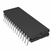
AD669SQ Analog Devices Inc, AD669SQ Datasheet - Page 7

AD669SQ
Manufacturer Part Number
AD669SQ
Description
IC,D/A CONVERTER,SINGLE,16-BIT,BICMOS,DIP,28PIN
Manufacturer
Analog Devices Inc
Series
DACPORT®r
Datasheet
1.AD669ANZ.pdf
(12 pages)
Specifications of AD669SQ
Rohs Status
RoHS non-compliant
Settling Time
10µs
Number Of Bits
16
Data Interface
Parallel
Number Of Converters
1
Voltage Supply Source
Dual ±
Power Dissipation (max)
625mW
Operating Temperature
-55°C ~ 125°C
Mounting Type
Through Hole
Package / Case
28-CDIP (0.600", 15.24mm)
Lead Free Status / RoHS Status
Available stocks
Company
Part Number
Manufacturer
Quantity
Price
REV. A
allows 5 V, 8.192 V and 10.24 V ranges to be used. For ex-
ample, by using the AD586 5 V reference, outputs of 0 V to
+5 V unipolar or 5 V bipolar can be realized. Using the
AD586 voltage reference makes it possible to operate the
AD669 off of 12 V supplies with 10% tolerances.
Figure 5 shows the AD669 using the AD586 5 V reference in
the bipolar configuration. This circuit includes two optional po-
tentiometers and one optional resistor that can be used to adjust
the gain, offset and bipolar zero errors in a manner similar to
that described in the BIPOLAR CONFIGURATION section.
Use –5.000000 V and +4.999847 as the output values.
Figure 5. Using the AD669 with the AD586 5 V Reference
GND
4
AD586
+V
R3
2
CC
V
TRIM
OUT
5
R
R2
S
6
5
9
A2
7
A1
R1
10
R2
10k
R5
100
R1
6
8
Figure 6. Using the AD669 with the AD688 High Precision 10 V Reference
50
R4
12
23
27
28
5
6
R6
4
L1
LDAC
REF IN
REF OUT
CS
11 13
AD688
(MSB)
DB15
–V
1
7
EE
3
+V
A3
A4
CC
2
AD669
+V
SPAN/BIP
16
3
14
15
1
2
LL
OFFSET
(LSB)
DB0
22
+V
–V
4
100
CC
EE
R1
24
26
25
LDAC
GND
OUTPUT
CS
L1
23
27
28
6
5
–7–
10k
USING THE AD669 WITH THE AD688 HIGH PRECISION
VOLTAGE REFERENCE
The AD669 is specified for gain drift from 15 ppm/ C to
25 ppm/ C (depending upon grade) using its internal 10 volt
reference. Since the internal reference contributes the vast ma-
jority of this drift, an external high precision voltage reference
will greatly improve performance over temperature. As shown in
Figure 6, the +10 volt output from the AD688 is used as the
AD669 reference. With a 3 ppm/ C drift over the industrial
temperature range, the AD688 will improve the gain drift by a
factor of 5 to a factor of 8 (depending upon the grade of the
AD669 being used). Using this combination may result in ap-
parent increases in initial gain error due to the differences
between the internal reference by which the device is laser
trimmed and the external reference with which the device is ac-
tually applied. The AD669 internal reference is specified to be
10 volts 20 mV whereas the AD688 is specified as 10 volts
parent initial gain error beyond the specified AD669 gain error.
The circuit shown in Figure 6 also makes use of the –10 V
AD688 output to allow the unipolar offset and gain to be ad-
justed to zero in the manner described in the UNIPOLAR
CONFIGURATION section.
10V REF
5 mV. This may result in an additional 5 mV (33 LSBs) of ap-
-V
(MSB)
DB15
1
EE
7
16-BIT LATCH
16-BIT LATCH
16-BIT DAC
+V
2
CC
AD669
+V
(LSB)
3
DB0
LL
22
4
AMP
10.05k
10k
26
25
24
R3
20k
R2
100
R4
10k
AD669
OUTPUT
0 TO +10V
GND


