AD679AJ Analog Devices Inc, AD679AJ Datasheet

A/D Converter (A-D) IC

AD679AJ

Manufacturer Part Number
AD679AJ
Description
A/D Converter (A-D) IC
Manufacturer
Analog Devices Inc
Datasheet

Specifications of AD679AJ

No. Of Bits
14 Bit
Mounting Type
Surface Mount
No. Of Channels
1
Interface Type
Parallel
Package / Case
44-PLCC
Rohs Status
RoHS non-compliant
Number Of Bits
14
Sampling Rate (per Second)
128k
Data Interface
Parallel
Number Of Converters
2
Power Dissipation (max)
745mw
Voltage Supply Source
Analog and Digital, Dual ±
Operating Temperature
-40°C ~ 85°C
Number Of Elements
1
Resolution
14Bit
Architecture
Flash
Sample Rate
128KSPS
Input Polarity
Unipolar/Bipolar
Input Type
Voltage
Rated Input Volt
10/±5V
Differential Input
No
Power Supply Requirement
Dual
Single Supply Voltage (typ)
Not RequiredV
Single Supply Voltage (min)
Not RequiredV
Single Supply Voltage (max)
Not RequiredV
Dual Supply Voltage (typ)
±12V
Dual Supply Voltage (min)
±11.4V
Dual Supply Voltage (max)
±12.6V
Power Dissipation
745mW
Integral Nonlinearity Error
±2LSB(Typ)
Operating Temp Range
-40C to 85C
Operating Temperature Classification
Industrial
Mounting
Surface Mount
Pin Count
44
Package Type
JLCC
Input Signal Type
Single-Ended
Lead Free Status / Rohs Status
Not Compliant

Available stocks

Company
Part Number
Manufacturer
Quantity
Price
Part Number:
AD679AJ
Manufacturer:
INT
Quantity:
4
Part Number:
AD679AJ
Manufacturer:
ADI
Quantity:
237
Part Number:
AD679AJZ
Manufacturer:
ADI
Quantity:
237
a
GENERAL DESCRIPTION
The AD679 is a complete, multipurpose 14-bit monolithic
analog-to-digital converter, consisting of a sample-and-hold am-
plifier (SHA), a microprocessor-compatible bus interface, a volt-
age reference, and clock generation circuitry.
The AD679 is specified for ac (or dynamic) parameters such as
S/N+D ratio, THD, and IMD, which are important in signal
processing applications. In addition, the AD679K, B, and T
grades are fully specified for dc parameters that are important in
measurement applications.
The 14 data bits are accessed in two read operations (8 + 6),
with left justification. Data format is straight binary for unipolar
mode and twos complement binary for bipolar mode. The input
has a full-scale range of 10 V with a full power bandwidth of
1 MHz and a full linear bandwidth of 500 kHz. High input
impedance (10 MΩ) allows direct connection to unbuffered
sources without signal degradation. Conversions can be initiated
either under microprocessor control or by an external clock
asynchronous to the system clock.
This product is fabricated on Analog Devices’ BiMOS process,
combining low power CMOS logic with high precision, low
noise bipolar circuits; laser-trimmed thin-film resistors provide
high accuracy. The converter utilizes a recursive subranging
algorithm that includes error correction and flash converter
circuitry to achieve high speed and resolution.
The AD679 operates from +5 V and ±12 V supplies and dissipates
560 mW (typ). The part is available in 28-lead plastic DIP,
ceramic DIP, and 44 J-leaded ceramic surface-mount packages.
REV. D
Information furnished by Analog Devices is believed to be accurate and
reliable. However, no responsibility is assumed by Analog Devices for its
use, nor for any infringements of patents or other rights of third parties that
may result from its use. No license is granted by implication or otherwise
under any patent or patent rights of Analog Devices. Trademarks and
registered trademarks are the property of their respective owners.
FEATURES
AC and DC Characterized and Specified
128k Conversions per Second
1 MHz Full Power Bandwidth
500 kHz Full Linear Bandwidth
78 dB S/N+D (K, B, T Grades)
Twos Complement Data Format (Bipolar Mode)
Straight Binary Data Format (Unipolar Mode)
10 M
8-Bit Bus Interface
On-Board Reference and Clock
10 V Unipolar or Bipolar Input Range
Pin Compatible with AD678 12-Bit, 200 kSPS ADC
MIL-STD-883 Compliant Versions Available
(K, B, T Grades)
Input Impedance
PRODUCT HIGHLIGHTS
1. COMPLETE INTEGRATION: The AD679 minimizes
2. SPECIFICATIONS: The AD679K, B, and T grades provide
3. EASE OF USE: The pinout is designed for easy board layout,
4. RELIABILITY: The AD679 utilizes Analog Devices’ mono-
5. UPGRADE PATH: The AD679 provides the same pinout as
6. The AD679 is available in versions compliant with MIL-
One Technology Way, P.O. Box 9106, Norwood, MA 02062-9106, U.S.A.
Tel: 781/329-4700
Fax: 781/326-8703
external component requirements by combining a high
speed sample-and-hold amplifier (SHA), ADC, 5 V refer-
ence, clock, and digital interface on a single chip. This
provides a fully specified sampling A/D function unattain-
able with discrete designs.
fully specified and tested ac and dc parameters. The AD679J,
A, and S grades are specified and tested for ac parameters; dc
accuracy specifications are shown as typicals. DC specifica-
tions (such as INL, gain, and offset) are important in control
and measurement applications. AC specifications (such as
S/N+D ratio, THD, and IMD) are of value in signal process-
ing applications.
and the two-read output provides compatibility with 8-bit
buses. Factory trimming eliminates the need for calibration
modes or external trimming to achieve rated performance.
lithic BiMOS technology. This ensures long-term reliability
compared to multichip and hybrid designs.
the 12-bit, 200 kSPS AD678 ADC.
STD-883. Refer to the Analog Devices Military Products
Databook or current AD679/883B data sheet for detailed
specifications.
FUNCTIONAL BLOCK DIAGRAM
Complete Sampling ADC
© 2004 Analog Devices, Inc. All rights reserved.
14-Bit 128 kSPS
AD679
www.analog.com

Related parts for AD679AJ

AD679AJ Summary of contents

Page 1

FEATURES AC and DC Characterized and Specified ( Grades) 128k Conversions per Second 1 MHz Full Power Bandwidth 500 kHz Full Linear Bandwidth 78 dB S/N+D ( Grades) Twos Complement Data Format (Bipolar Mode) Straight ...

Page 2

AD679–SPECIFICATIONS ( MIN AC SPECIFICATIONS unless otherwise noted) Parameter SIGNAL-TO-NOISE AND DISTORTION (S/N+D) RATIO –0.5 dB Input (Referred to –0 dB Input) –20 dB Input (Referred to –20 dB Input) –60 dB Input (Referred to –60 dB Input) ...

Page 3

DC SPECIFICATIONS ( MIN Parameter TEMPERATURE RANGE J, K Grades A, B Grades S, T Grades ACCURACY Resolution Integral Nonlinearity (INL) Differential Nonlinearity (DNL) 1 Unipolar Zero Error (@ 25°C) 1 Bipolar Zero Error (@ 25° ...

Page 4

AD679 TIMING SPECIFICATIONS Parameter Symbol SC Delay t SC Conversion Time Conversion Rate t CR Convert Pulse Width t CP Aperture Delay t AD Status Delay Access Time Float Delay ...

Page 5

... Temperature Model AD679JN AD679KN AD679JD AD679KD AD679AD AD679BD AD679SD AD679TD AD679AJ AD679BJ 3 AD679SD/883B NOTES 1 For parallel read (14-bits) interface to 16-bit buses, see AD779 Plastic DIP Ceramic DIP J-Leaded Ceramic Chip Carrier. 3 For details, grade, and package offerings screened in accordance with MIL-STD-883, refer to the Analog Devices Military Products Databook or the current AD679/883B data sheet ...

Page 6

AD679 DIP Package EOCEN AIN 6 23 AD679 AGND 7 22 TOP VIEW (Not to Scale) REF 8 21 OUT REF BIPOFF ...

Page 7

DEFINITIONS OF SPECIFICATIONS Nyquist Frequency An implication of the Nyquist sampling theorem, the Nyquist frequency of a converter is the input frequency that is one-half the sampling frequency of the converter. Signal-to-Noise and Distortion (S/N+D) Ratio S/N+D is the ratio ...

Page 8

AD679 –Typical Performance Characteristics INPUT FREQUENCY (Hz) TPC 1. Harmonic Distortion vs. Input Frequency (–0.5 dB Input) INPUT FREQUENCY (Hz) TPC 2. Total Harmonic Distortion vs. Input Frequency and Amplitude INPUT FREQUENCY (Hz) TPC 3. S/(N+D) vs. Input Frequency and ...

Page 9

CONVERSION CONTROL In synchronous mode (SYNC = HIGH), both chip select (CS) and start convert (SC) must be brought LOW to start a conver- sion. CS should be LOW t before SC is brought LOW asynchronous mode (SYNC ...

Page 10

AD679 INPUT CONNECTIONS AND CALIBRATION The high (10 MΩ) input impedance of the AD679 eases the task of interfacing to high source impedances or multiplexer channel-to-channel mismatches 300 Ω. The 10 V p-p full-scale input range accepts ...

Page 11

Analog signals should be routed as far as possible from digital signals and should cross them at right angles. The AD679 incorporates several ...

Page 12

AD679 INTERFACING THE AD679 TO MICROPROCESSORS The I/O capabilities of the AD679 allow direct interfacing to general-purpose and DSP microprocessor buses. The asynchro- nous conversion control feature allows complete flexibility and control with minimal external hardware. The following examples illustrate ...

Page 13

AD679 to Analog Devices ADSP-2100A Figure 12 demonstrates the AD679 interfaced to an ADSP-2100A. With a clock frequency of 12.5 MHz, and instruction execution in one 80 ns cycle, the digital signal processor supports the AD679 data memory interface with ...

Page 14

AD679 28-Lead Side-Brazed Ceramic Dual In-Line Package [SBDIP] 0.005 (0.13) MIN PIN 1 0.085 (2.16) MAX 0.200 (5.08) 0.125 (3.18) 0.005 (0.13) MIN PIN 1 0.085 (2.16) MAX 0.200 (5.08) 0.125 (3.18) OUTLINE DIMENSIONS (D-28) Dimensions shown in inches and ...

Page 15

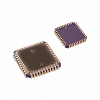
Ceramic Leaded Chip Carrier, J-Formed Leads [JLCC] 0.078 (1.98) 0.054 (1.37) 0.025 (0.64) MIN 0.032 (0.81) 0.020 (0.51) 0.050 0.650 (16.51) (1.27) 0.610 (15.49) 0.023 (0.58) 0.013 (0.33) 0.135 (3.43) 0.100 (2.54) CONTROLLING DIMENSIONS ARE IN INCHES; MILLIMETERS DIMENSIONS ...

Page 16

–16– ...

Related keywords