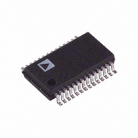
AD7714ARS-3 Analog Devices Inc, AD7714ARS-3 Datasheet - Page 29

AD7714ARS-3
Manufacturer Part Number
AD7714ARS-3
Description
A/D Converter (A-D) IC
Manufacturer
Analog Devices Inc
Datasheet
1.AD7714YNZ.pdf
(40 pages)
Specifications of AD7714ARS-3
No. Of Bits
24 Bit
Mounting Type
Surface Mount
Features
24-Bit, 3V/5V Sigma-Delta ADC, 5-Channels
No. Of Channels
6
Interface Type
Serial
Package / Case
28-SSOP
Rohs Status
RoHS non-compliant
Number Of Bits
24
Sampling Rate (per Second)
1k
Data Interface
DSP, MICROWIRE™, QSPI™, Serial, SPI™
Number Of Converters
1
Power Dissipation (max)
7mW
Voltage Supply Source
Analog and Digital
Operating Temperature
-40°C ~ 85°C
For Use With
EVAL-AD7714-3EBZ - BOARD EVALUATION FOR AD7714
Lead Free Status / RoHS Status
DIGITAL INTERFACE
The AD7714’s programmable functions are controlled using a
set of on-chip registers as previously outlined. Data is written to
these registers via the part’s serial interface, and read access to
the on-chip registers is also provided by this interface. All com-
munications to the part must start with a write operation to the
Communications Register. After power-on or RESET, the de-
vice expects a write to its Communications Register. The data
written to this register determines whether the next operation to
the part is a read or a write operation and also determines to
which register this read or write operation occurs. Therefore,
write access to any of the other registers on the part starts with a
write operation to the Communications Register followed by a
write to the selected register. A read operation from any register
on the part (including the output data register) starts with a
write operation to the Communications Register followed by a
read operation from the selected register.
The AD7714’s serial interface consists of five signals, CS,
SCLK, DIN, DOUT and DRDY. The DIN line is used for
transferring data into the on-chip registers while the DOUT line
is used for accessing data from the on-chip registers. SCLK is
the serial clock input for the device and all data transfers (either
on DIN or DOUT) take place with respect to this SCLK signal.
The DRDY line is used as a status signal to indicate when data
is ready to be read from the AD7714’s data register. DRDY
goes low when a new data word is available in the output regis-
ter. It is reset high when a read operation from the data register
is complete. It also goes high prior to the updating of the output
register to indicate when not to read from the device to ensure
that a data read is not attempted while the register is being
updated. CS is used to select the device. It can be used to de-
code the AD7714 in systems where a number of parts are con-
nected to the serial bus.
REV. C
DRDY
DOUT
SCLK
SCLK
CS
DIN
CS
t
5
t
12
t
t
Figure 7. Write Cycle Timing Diagram (POL = 1)
4
Figure 6. Read Cycle Timing Diagram (POL = 1)
11
t
3
MSB
MSB
t
13
t
t
6
14
t
t
7
15
–29–
The AD7714 serial interface can operate in three-wire mode by
tying the CS input low. In this case, the SCLK, DIN and
DOUT lines are used to communicate with the AD7714 and
the status of DRDY can be obtained by interrogating the MSB
of the Communications Register.
Figures 6 and 7 show timing diagrams for interfacing to the
AD7714 with CS used to decode the part. Figure 6 is for a read
operation from the AD7714’s output shift register, while Figure
7 shows a write operation to the input shift register. Both dia-
grams are for the POL input at a logic high; for operation with
the POL input at a logic low simply invert the SCLK waveform
shown in the diagrams. It is possible to read the same data
twice from the output register even though the DRDY line
returns high after the first read operation. Care must be taken,
however, to ensure that the read operations have been com-
pleted before the next output update is about to take place.
The serial interface can be reset by exercising the RESET input
on the part. It can also be reset by writing a series of 1s on the
DIN input. If a logic 1 is written to the AD7714 DIN line for at
least 32 serial clock cycles the serial interface is reset. This
ensures in three-wire systems that if the interface gets lost, either
via a software error or by some glitch in the system, it can be
reset back into a known state. This state returns the interface to
where the AD7714 is expecting a write operation to the Com-
munications Register. This operation does not in itself reset the
contents of any registers but since the interface was lost, the
information that was written to any of the registers is unknown
and it is advisable to set up all registers again.
LSB
LSB
t
10
t
9
t
t
8
16
AD7714
2


