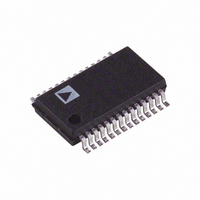
AD7714ARSZ-5 Analog Devices Inc, AD7714ARSZ-5 Datasheet - Page 14

AD7714ARSZ-5
Manufacturer Part Number
AD7714ARSZ-5
Description
28-BIT SIGMA DELTA A/D IC
Manufacturer
Analog Devices Inc
Datasheet
1.AD7714YNZ.pdf
(40 pages)
Specifications of AD7714ARSZ-5
Rohs Compliant
YES
Number Of Bits
24
Sampling Rate (per Second)
1k
Data Interface
DSP, MICROWIRE™, QSPI™, Serial, SPI™
Number Of Converters
1
Power Dissipation (max)
7mW
Voltage Supply Source
Analog and Digital
Operating Temperature
-40°C ~ 85°C
Mounting Type
Surface Mount
Package / Case
28-SSOP (0.200", 5.30mm Width)
Lead Free Status / RoHS Status
Lead free / RoHS Compliant
For Use With
EVAL-AD7714-3EBZ - BOARD EVALUATION FOR AD7714
Lead Free Status / RoHS Status
Lead free / RoHS Compliant
Available stocks
Company
Part Number
Manufacturer
Quantity
Price
Company:
Part Number:
AD7714ARSZ-5
Manufacturer:
YAGEO
Quantity:
460 000
Part Number:
AD7714ARSZ-5
Manufacturer:
ADI/亚德诺
Quantity:
20 000
AD7714
ON-CHIP REGISTERS
The AD7714 contains eight on-chip registers which can be accessed via the serial port of the part. The first of these is a Communica-
tions Register which controls the channel selection, decides whether the next operation is a read or write operation and also decides
which register the next read or write operation accesses. All communications to the part must start with a write operation to the
Communications Register. After power-on or RESET, the device expects a write to its Communications Register. The data written
to this register determines whether the next operation to the part is a read or a write operation and also determines to which register
this read or write operation occurs. Therefore, write access to any of the other registers on the part starts with a write operation to the
Communications Register followed by a write to the selected register. A read operation from any other register on the part (including
the output data register) starts with a write operation to the Communications Register followed by a read operation from the selected
register. The communications register also controls channel selection and the DRDY status is also available by reading from the
Communications Register. The second register is a Mode Register which determines calibration mode and gain setting. The third
register is labelled the Filter High Register and this determines the word length, bipolar/unipolar operation and contains the upper 4
bits of the filter selection word. The fourth register is labelled the Filter Low Register and contains the lower 8 bits of the filter selec-
tion word. The fifth register is a Test Register which is accessed when testing the device. The sixth register is the Data Register from
which the output data from the part is accessed. The final registers allow access to the part’s calibration registers. The Zero Scale
Calibration Register allows access to the zero scale calibration coefficients for the selected input channel while the Full Scale Calibra-
tion Register allows access to the full scale calibration coefficients for the selected input channel. The registers are discussed in more
detail in the following sections.
Communications Register (RS2-RS0 = 0, 0, 0)
The Communications Register is an 8-bit register from which data can either be read or to which data can be written. All communi-
cations to the part must start with a write operation to the Communications Register. The data written to the Communications Reg-
ister determines whether the next operation is a read or write operation and to which register this operation takes place. Once the
subsequent read or write operation to the selected register is complete, the interface returns to where it expects a write operation to
the Communications Register. This is the default state of the interface, and on power-up or after a RESET, the AD7714 is in this
default state waiting for a write operation to the Communications Register. In situations where the interface sequence is lost, if a
write operation of sufficient duration (containing at least 32 serial clock cycles) takes place with DIN high, the AD7714 returns to
this default state. Table V outlines the bit designations for the Communications Register.
0/DRDY
RS2–RS0
0/DRDY
Register Selection Bits. RS2 is the MSB of the three selection bits. The three bits select to which one of eight on-chip
For a write operation, a 0 must be written to this bit so that the write operation to the Communications Register
actually takes place. If a 1 is written to this bit, the part will not clock on to subsequent bits in the register. It will stay
at this bit location until a 0 is written to this bit. Once a 0 is written to this bit, the next 7 bits will be loaded to the
Communications Register. For a read operation, this bit provides the status of the DRDY flag from the part. The
status of this bit is the same as the DRDY output pin.
registers the next read or write operation takes place as shown in Table VI along with the register size.
0
0
0
1
1
1
1
RS2
0
RS1
0
0
1
1
0
0
1
1
RS2
RS0
0
1
0
1
0
1
0
1
RS1
Register
Communications Register
Mode Register
Filter High Register
Filter Low Register
Test Register
Data Register
Zero-Scale Calibration Register
Full-Scale Calibration Register
Table V. Communications Register
Table VI. Register Selection
RS0
–14–
R/W
Register Size
8 Bits
8 Bits
8 Bits
8 Bits
8 Bits
16 Bits or 24 Bits
24 Bits
24 Bits
CH2
CH1
CH0
REV. C


