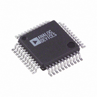
AD7865BSZ-1 Analog Devices Inc, AD7865BSZ-1 Datasheet - Page 6

AD7865BSZ-1
Manufacturer Part Number
AD7865BSZ-1
Description
4 CH. SIMULTANEOUS BIPOLAR,14-B ADC I.C.
Manufacturer
Analog Devices Inc
Datasheet
1.AD7865AS-2REEL.pdf
(19 pages)
Specifications of AD7865BSZ-1
Number Of Bits
14
Sampling Rate (per Second)
350k
Data Interface
Parallel
Number Of Converters
1
Power Dissipation (max)
160mW
Voltage Supply Source
Analog and Digital
Operating Temperature
-40°C ~ 85°C
Mounting Type
Surface Mount
Package / Case
44-MQFP, 44-PQFP
Lead Free Status / RoHS Status
Lead free / RoHS Compliant
Available stocks
Company
Part Number
Manufacturer
Quantity
Price
Company:
Part Number:
AD7865BSZ-1
Manufacturer:
ADI
Quantity:
364
Company:
Part Number:
AD7865BSZ-1
Manufacturer:
Analog Devices Inc
Quantity:
10 000
Part Number:
AD7865BSZ-1
Manufacturer:
ADI/亚德诺
Quantity:
20 000
Company:
Part Number:
AD7865BSZ-1REEL
Manufacturer:
Analog Devices Inc
Quantity:
10 000
AD7865
Pin
1
2
3
4
5
6
7
8
9, 10
11
12
13–16
17
18–21
22
23
Mnemonic
BUSY
FRSTDATA
CONVST
CS
RD
WR
CLK IN/SL1
INT/EXT CLK/SL2
SL3, SL4
H/S SEL
AGND
V
AGND
V
STBY
AGND
IN4x
IN2x
, V
, V
IN3x
IN1x
Description
Busy Output. The busy output is triggered high by the rising edge of CONVST and remains
high until conversion is completed on all selected channels.
First Data Output. FRSTDATA is a logic output which, when high, indicates that the Output
Data Register Pointer is addressing Register 1—See Accessing the Output Data Registers.
Convert Start Input. Logic Input. A low-to-high transition on this input puts all track/holds
into their hold mode and starts conversion on the selected channels. In addition, the state of
the Channel Sequence Selection is also latched on the rising edge of CONVST.
Chip Select Input. Active low logic input. The device is selected when this input is active.
Read Input. Active low logic input which is used in conjunction with CS low to enable the
data outputs. Ensure the WR pin is at logic high while performing a read operation.
Write Input. A rising edge on the WR input, with CS low and RD high, latches the logic state
on DB0 to DB3 into the channel select register.
Conversion Clock Input/Hardware Channel Select. The function of this pin depends upon the
H/S SEL input. When the H/S SEL input is high (choosing software control of the channel
selection sequence), this pin assumes its CLK IN function. CLK IN is an externally applied
clock (that is only necessary when INT/EXT CLK is high) this allows the user to control the
conversion rate of the AD7865. Each conversion needs 16 clock cycles in order for the conver-
sion to be completed. The clock should have a duty cycle that is no greater than 60/40. See
Using an External Clock.
When the H/S SEL input is low (choosing hardware control of the channel conversion se-
quence), this pin assumes its Hardware Channel Select function. The SL1 input determines
whether Channel 1 is included in the channel conversion sequence. The selection is latched
on the rising edge of CONVST. See Selecting a Conversion Sequence.
Internal/External Clock/Hardware Channel Select. The function of this pin depends upon the
H/S SEL input. When the H/S SEL input is high (choosing software control of the channel
selection sequence), this pin assumes its INT/EXT CLK function. When INT/EXT CLK is at
a Logic 0, the AD7865 uses its internally generated master clock. When INT/EXT CLK is at
Logic 1, the master clock is generated externally to the device and applied to CLK IN.
When the H/S SEL input is low (choosing hardware control of the channel conversion sequence),
this pin assumes its Hardware Channel Select function. The SL2 input determines whether
Channel 2 is included in the channel conversion sequence. The selection is latched on the
rising edge of CONVST. When H/S is at Logic 1 these pins have no function and can be tied
to Logic 1 or Logic 0. See Selecting a Conversion Sequence.
Hardware Channel Select. When the H/S SEL input is at Logic 0, the SL3 input determines
whether Channel 3 is included in the channel conversion sequence while SL4 determines
whether Channel 4 is included in the channel conversion sequence. When the pin is at Logic
1, the channel is included in the conversion sequence. When the pin is at Logic 0, the channel
is excluded from the conversion sequence. The selection is latched on the rising edge of
CONVST. See Selecting a Conversion Sequence.
Hardware/Software Select Input. When this pin is at a Logic 0, the AD7865 conversion
sequence selection is controlled via the SL1–SL4 input pins and runs off an internal clock.
When this pin is at Logic 1, the conversion sequence is controlled via the channel select regis-
ter and allows the ADC to run with an internal or external clock. See Selecting a Conversion
Sequence.
Analog Ground. General Analog Ground. This AGND pin should be connected to the system’s
AGND plane.
Analog Inputs. See Analog Input section.
Analog Ground. Analog Ground reference for the attenuator circuitry. This AGND pin
should be connected to the system’s AGND plane.
Analog Inputs. See Analog Input section.
Standby Mode Input. This pin is used to put the device into the power save or standby mode.
The STBY input is high for normal operation and low for standby operation.
Analog Ground. General Analog Ground. This AGND pin should be connected to the
system’s AGND plane.
PIN FUNCTION DESCRIPTIONS


