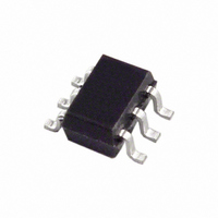
AD8029AKSZ-REEL Analog Devices Inc, AD8029AKSZ-REEL Datasheet

AD8029AKSZ-REEL
Specifications of AD8029AKSZ-REEL
Available stocks
Related parts for AD8029AKSZ-REEL
AD8029AKSZ-REEL Summary of contents
Page 1
FEATURES Low power 1.3 mA supply current/amplifier High speed 125 MHz, –3 dB bandwidth (G = +1) 60 V/µs slew rate 80 ns settling time to 0.1% Rail-to-rail input and output No phase reversal, inputs 200 mV beyond rails Wide ...
Page 2
AD8029/AD8030/AD8040 TABLE OF CONTENTS Specifications..................................................................................... 3 Specifications with ±5 V Supply ................................................. 3 Specifications with +5 V Supply ................................................. 4 Specifications with +3 V Supply ................................................. 5 Absolute Maximum Ratings............................................................ 6 Maximum Power Dissipation ..................................................... 6 Typical Performance Characteristics ............................................. ...
Page 3
SPECIFICATIONS SPECIFICATIONS WITH ±5 V SUPPLY Table ± 25° + Parameter DYNAMIC PERFORMANCE –3 dB Bandwidth Bandwidth for 0.1 dB Flatness Slew Rate Settling Time to 0.1% NOISE/DISTORTION ...
Page 4
AD8029/AD8030/AD8040 SPECIFICATIONS WITH +5 V SUPPLY Table 25° + Parameter DYNAMIC PERFORMANCE –3 dB Bandwidth Bandwidth for 0.1 dB Flatness Slew Rate Settling Time to 0.1% NOISE/DISTORTION ...
Page 5
SPECIFICATIONS WITH +3 V SUPPLY Table 25° + Parameter DYNAMIC PERFORMANCE –3 dB Bandwidth Bandwidth for 0.1 dB Flatness Slew Rate Settling Time to 0.1% NOISE/DISTORTION PERFORMANCE ...
Page 6
AD8029/AD8030/AD8040 ABSOLUTE MAXIMUM RATINGS Table 4. AD8029/AD8030/AD8040 Stress Ratings Parameter Rating Supply Voltage 12.6 V Power Dissipation See Figure 6 Common-Mode Input Voltage ±V Differential Input Voltage ±1.8 V Storage Temperature –65°C to +125°C Operating Temperature Range –40°C to +125°C ...
Page 7
TYPICAL PERFORMANCE CHARACTERISTICS Default Conditions 25° –1 – +10 – 9kΩ 1kΩ –4 – – ...
Page 8
AD8029/AD8030/AD8040 0.1V p-p O 20pF 4 10pF 3 2 5pF 1 0 –1 0pF –2 –3 –4 –5 –6 –7 – 100 FREQUENCY (MHz) Figure 13. Small Signal Frequency Response for ...
Page 9
p-p OUT R = 1kΩ –45 L SECOND HARMONIC: SOLID LINE THIRD HARMONIC: DASHED LINE –55 – +3V S –75 – + ± –95 –105 ...
Page 10
AD8029/AD8030/AD8040 100 ±2. –25 –50 –75 25mV/DIV –100 TIME (ns) Figure 25. Small Signal Transient Response 2 p ±2.5V 2.0 S 1.5 1.0 2V ...
Page 11
V – 2V OUT IN V (500mV/DIV) OUT –1V Figure 31. Long-Term Settling Time –20 –30 –40 –50 –60 –70 –80 –90 –100 1k 10k 100k 1M 10M FREQUENCY (Hz) Figure 32. Common-Mode Rejection Ratio vs. Frequency –20 G ...
Page 12
AD8029/AD8030/AD8040 2 1.5 1.0 0.5 0 –0.5 –1.0 –1.5 –2.0 –2.5 – INPUT COMMON-MODE VOLTAGE (V) Figure 37. Input Bias Current vs. Input Common-Mode ...
Page 13
DISABLE = LOW 100k 10k 1k 100 10 1 100k 1M 10M 100M FREQUENCY (Hz) Figure 43. AD8029 Output Impedance vs. Frequency, Disabled 0.5 LOAD RESISTANCE TIED TO MIDSUPPLY 0.4 0.3 0.2 V – 0.1 = ...
Page 14
AD8029/AD8030/AD8040 1.5 DISABLE (–0.5V TO –2V) 1.0 0 100Ω 1kΩ 10kΩ L –0.5 –1.0 –1 100 150 200 TIME (ns) Figure 47. AD8029 DISABLE Turn-Off Timing 1.5 DISABLE (–2V ...
Page 15
THEORY OF OPERATION DISABLE TO DISABLE AD8029 ONLY IN– IN+ The AD8029 (single), AD8030 (dual), and AD8040 (quad) are rail-to-rail input and output amplifiers fabricated using Analog Devices’ XFCB process. The XFCB process enables the AD8029/ AD8030/AD8040 to operate on ...
Page 16
AD8029/AD8030/AD8040 APPLICATIONS WIDEBAND OPERATION 10µF C1 0.1µ – AD8029 0.1µ ||R 10µ –V S Figure 51. Wideband Non-inverting Gain Configuration R F ...
Page 17
Table 5. Effect of Load on Performance Noninverting Gain (kΩ) (kΩ) (kΩ 2.5 2.5 2 ...
Page 18
AD8029/AD8030/AD8040 CIRCUIT CONSIDERATIONS PCB Layout High speed op amps require careful attention to PCB layout to achieve optimum performance. Particular care must be exercised to minimize lead lengths of the bypass capacitors. Excess lead inductance can influence the frequency response ...
Page 19
OUTLINE DIMENSIONS 5.00 (0.1968) 4.80 (0.1890 6.20 (0.2440) 4.00 (0.1574) 5.80 (0.2284) 3.80 (0.1497 1.27 (0.0500) BSC 1.75 (0.0688) 1.35 (0.0532) 0.25 (0.0098) 0.10 (0.0040) 0.51 (0.0201) COPLANARITY 0.25 (0.0098) 0.31 (0.0122) SEATING 0.10 0.17 (0.0067) ...
Page 20
AD8029/AD8030/AD8040 ORDERING GUIDE Model Minimum Ordering Quantity AD8029AR 1 AD8029AR-REEL 2,500 AD8029AR-REEL7 1,000 AD8029AKS-R2 250 AD8029AKS-REEL 10,000 AD8029AKS-REEL7 3,000 AD8030AR 1 AD8030AR-REEL 2,500 AD8030AR-REEL7 1,000 AD8030ARJ-R2 250 AD8030ARJ-REEL 10,000 AD8030ARJ-REEL7 3,000 AD8040AR 1 AD8040AR-REEL 2500 AD8040AR-REEL7 1000 AD8040ARU 1 AD8040ARU-REEL ...


