AD8045ACPZ-REEL7 Analog Devices Inc, AD8045ACPZ-REEL7 Datasheet
AD8045ACPZ-REEL7
Specifications of AD8045ACPZ-REEL7
AD8045ACPZ-REEL7TR
Available stocks


Related parts for AD8045ACPZ-REEL7


AD8045ACPZ-REEL7 Summary of contents
Page 1
FEATURES Ultralow distortion SFDR −101 dBc @ 5 MHz −90 dBc @ 20 MHz −63 dBc @ 70 MHz Third-order intercept 43 dBm @ 10 MHz Low noise 3 nV/√Hz 3 pA/√Hz High speed 1 GHz, −3 dB bandwidth (G ...
Page 2
AD8045 TABLE OF CONTENTS Specifications with ±5 V Supply ..................................................... 3 Specifications with +5 V Supply ..................................................... 4 Absolute Maximum Ratings............................................................ 5 Thermal Resistance ...................................................................... 5 ESD Caution.................................................................................. 5 Pin Configurations and Function Descriptions ........................... 6 Typical Performance Characteristics ............................................. ...
Page 3
SPECIFICATIONS WITH ±5 V SUPPLY T = 25° + 100 Ω kΩ to ground, unless noted otherwise. Exposed paddle must be floating or connected to − Table 1. Parameter DYNAMIC ...
Page 4
AD8045 SPECIFICATIONS WITH +5 V SUPPLY T = 25° + 100 Ω kΩ to midsupply, unless otherwise noted. Exposed paddle must be floating or connected to − Table 2. Parameter ...
Page 5
ABSOLUTE MAXIMUM RATINGS Table 3. Parameter Rating Supply Voltage 12.6 V Power Dissipation See Figure 4 Common-Mode Input Voltage −V ±V Differential Input Voltage S Exposed Paddle Voltage −V Storage Temperature −65°C to +125°C Operating Temperature Range −40°C to +125°C ...
Page 6
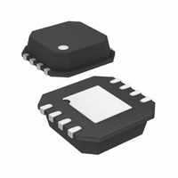
AD8045 PIN CONFIGURATIONS AND FUNCTION DESCRIPTIONS AD8045 OUTPUT 6 3 BOTTOM VIEW (Not to Scale CONNECT Figure 5. SOIC Pin Configuration Note: The exposed paddle must be ...
Page 7
TYPICAL PERFORMANCE CHARACTERISTICS ± 1kΩ –1 – +10 –3 –4 –5 –6 – FREQUENCY (MHz) Figure 7. Small Signal Frequency Response for Various Gains ...
Page 8
AD8045 –1 –2 –3 – ±2.5V S –5 –6 –7 –8 –9 –10 10 100 FREQUENCY (MHz) Figure 13. Large Signal Frequency Response for Various Supplies –1 –2 –3 – ...
Page 9
±5V S – p-p OUT R = 100Ω L – 100Ω S –50 –60 –70 HD2 SOIC –80 –90 HD2 LFCSP –100 HD3 SOIC AND LFCSP –110 0.1 1 ...
Page 10
AD8045 – ± 150Ω – 100Ω 10MHz –60 HD2 LFCSP –70 HD2 SOIC –80 –90 –100 HD3 SOIC AND LFCSP –110 ...
Page 11
+ 1kΩ – 100Ω 10MHz –60 HD3 SOIC AND LFCSP –70 –80 –90 –100 HD2 LFCSP –110 0.5 1.0 1.5 2.0 OUTPUT VOLTAGE (V p-p) ...
Page 12
AD8045 0.20 18pF 0.15 0.10 0pF 0.05 0 –0.05 –0. –0. ± 1kΩ L –0. TIME (ns) Figure 37. Small Signal Transient Response with Capacitive Load 3 V ...
Page 13
× INPUT ± 5MHz OUTPUT 1 0 –1 –2 –3 –4 –5 – 100 120 140 TIME (ns) Figure 43. Output ...
Page 14
AD8045 1000 ±5V S 100 10 1 0.1 0. FREQUENCY (MHz) Figure 49. Output Impedance vs. Frequency FREQUENCY (MHz) Figure ...
Page 15
I – ±5V –1 –1 ± –2.0 –2.2 I – –2 –2.6 –2.8 –3.0 –40 ...
Page 16
AD8045 CIRCUIT CONFIGURATIONS WIDEBAND OPERATION Figure 61 and Figure 62 show the recommended circuit configurations for noninverting and inverting amplifiers. In unity gain (G = +1) applications, R helps to reduce high S frequency peaking not needed for ...
Page 17
THEORY OF OPERATION The AD8045 is a high speed voltage feedback amplifier fabri- cated on ADI’s second generation eXtra Fast Complementary Bipolar (XFCB) process. An H-bridge input stage is used to attain a 1400 V/µs slew rate and low distortion ...
Page 18
AD8045 OUTPUT NOISE Figure 66 shows the contributors to the noise at the output of a noninverting configuration – Figure 66. ...
Page 19
APPLICATIONS LOW DISTORTION PINOUT The AD8045 LFCSP package features Analog Devices new low distortion pinout. The new pinout provides two advantages over the traditional pinout. First, improved second harmonic distortion performance, which is accomplished by the physical separation of the ...
Page 20
AD8045 0 –20 –40 –60 –80 –100 –120 FREQUENCY (MHz) Figure 69. Single-Tone FFT MHz, Sample Rate = 65 MSPS IN Shown in the First Nyquist Zone 90 MHZ ACTIVE LOW-PASS FILTER ...
Page 21
CH1 50.0mV M4.00ns A CH1 Figure 71. Small Signal Transient Response of 90 MHz LPF R1 R2 249Ω 249Ω INPUT 49.9Ω 7.1pF R4 499Ω 1 0.00V CH1 500mV Figure 72. Large Signal Transient Response of 90 ...
Page 22
AD8045 PRINTED CIRCUIT BOARD LAYOUT Laying out the printed circuit board (PCB) is usually the last step in the design process and often proves to be one of the most critical. A brilliant design can be rendered useless because of ...
Page 23
EXPOSED PADDLE The AD8045 features an exposed paddle, which lowers the thermal resistance by 25% compared to a standard SOIC plastic package. The exposed paddle of the AD8045 is internally con- nected to the negative power supply pin. Therefore, when ...
Page 24
... AD8045ACP-REEL 5,000 AD8045ACP-REEL7 1,500 1 AD8045ACPZ-R2 250 1 AD8045ACPZ-REEL 5,000 1 AD8045ACPZ-REEL7 1,500 Pb-free part. © 2004 Analog Devices, Inc. All rights reserved. Trademarks and registered trademarks are the property of their respective owners. 5.00 (0.197) BOTTOM VIEW 4.90 (0.193) 4.80 (0.189) 4.00 (0.157) 3.90 (0.154) 3 ...