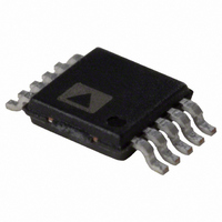
AD8250ARMZ-RL Analog Devices Inc, AD8250ARMZ-RL Datasheet - Page 17

AD8250ARMZ-RL
Manufacturer Part Number
AD8250ARMZ-RL
Description
IC,Instrumentation Amplifier,SINGLE,CMOS,TSSOP,10PIN,PLASTIC
Manufacturer
Analog Devices Inc
Series
iCMOS®r
Datasheet
1.AD8250-EVALZ.pdf
(24 pages)
Specifications of AD8250ARMZ-RL
Amplifier Type
Instrumentation
Number Of Circuits
1
Output Type
Push-Pull
Slew Rate
25 V/µs
-3db Bandwidth
10MHz
Current - Input Bias
5nA
Voltage - Input Offset
70µV
Current - Supply
4.1mA
Current - Output / Channel
37mA
Voltage - Supply, Single/dual (±)
10 V ~ 30 V, ±5 V ~ 15 V
Operating Temperature
-40°C ~ 85°C
Mounting Type
Surface Mount
Package / Case
10-MSOP, Micro10™, 10-uMAX, 10-uSOP
Lead Free Status / RoHS Status
Lead free / RoHS Compliant
For Use With
AD8250-EVALZ - BOARD EVALUATION AD8250
Gain Bandwidth Product
-
Lead Free Status / RoHS Status
Lead free / RoHS Compliant
Available stocks
Company
Part Number
Manufacturer
Quantity
Price
Part Number:
AD8250ARMZ-RL
Manufacturer:
ADI/亚德诺
Quantity:
20 000
POWER SUPPLY REGULATION AND BYPASSING
The AD8250 has high PSRR. However, for optimal performance,
a stable dc voltage should be used to power the instrumentation
amplifier. Noise on the supply pins can adversely affect per-
formance. As in all linear circuits, bypass capacitors must be
used to decouple the amplifier.
Place a 0.1 μF capacitor close to each supply pin. A 10 μF tantalum
capacitor can be used farther away from the part (see Figure 51)
and, in most cases, it can be shared by other precision integrated
circuits.
INPUT BIAS CURRENT RETURN PATH
The AD8250 input bias current must have a return path to its
local analog ground. When the source, such as a thermocouple,
cannot provide a return current path, one should be created
(see Figure 52).
Figure 51. Supply Decoupling, REF, and Output Referred to Ground
DGND
+IN
–IN
AD8250
+V
–V
S
S
WR
DGND
A1
0.1µF
0.1µF
A0
REF
10µF
10µF
LOAD
OUT
Rev. B | Page 17 of 24
INPUT PROTECTION
All terminals of the AD8250 are protected against ESD. Note
that 2.2 kΩ series resistors precede the ESD diodes as shown in
Figure 47. The resistors limit current into the diodes and allow
for dc overload conditions 13 V above the positive supply and
13 V below the negative supply. An external resistor should be
used in series with each input to limit current for voltages greater
than 13 V beyond either supply rail. In either scenario, the
AD8250 safely handles a continuous 6 mA current at room
temperature. For applications where the AD8250 encounters
extreme overload voltages, external series resistors and low
leakage diode clamps, such as BAV199Ls, FJH1100s, or SP720s,
should be used.
CAPACITIVELY COUPLED
C
C
THERMOCOUPLE
TRANSFORMER
INCORRECT
AD8250
+V
AD8250
–V
AD8250
+V
–V
+V
–V
S
S
S
S
S
S
Figure 52. Creating an I
REF
REF
REF
f
HIGH-PASS
CAPACITIVELY COUPLED
=
BIAS
2πRC
10MΩ
1
Return Path
C
C
THERMOCOUPLE
TRANSFORMER
R
R
CORRECT
AD8250
AD8250
AD8250
+V
–V
+V
–V
+V
–V
S
S
S
S
S
S
AD8250
REF
REF
REF


