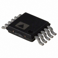
AD8253ARMZ-RL Analog Devices Inc, AD8253ARMZ-RL Datasheet

AD8253ARMZ-RL
Specifications of AD8253ARMZ-RL
Related parts for AD8253ARMZ-RL
AD8253ARMZ-RL Summary of contents
Page 1
FEATURES Small package: 10-lead MSOP Programmable gains: 1, 10, 100, 1000 Digital or pin-programmable gain setting Wide supply: ± ±15 V Excellent dc performance High CMRR: 100 dB (minimum 100 Low gain drift: 10 ppm/°C (maximum) ...
Page 2
AD8253 TABLE OF CONTENTS Features .............................................................................................. 1 Applications ....................................................................................... 1 General Description ......................................................................... 1 Functional Block Diagram .............................................................. 1 Revision History ............................................................................... 2 Specifications ..................................................................................... 3 Timing Diagram ........................................................................... 5 Absolute Maximum Ratings ............................................................ 6 Maximum Power Dissipation ..................................................... 6 ...
Page 3
SPECIFICATIONS +V = +15 V, −V = − REF Table 2. Parameter COMMON-MODE REJECTION RATIO (CMRR) CMRR with 1 kΩ Source Imbalance ...
Page 4
AD8253 Parameter Settling Time 0.001 =100 G = 1000 Slew Rate 100 G = 1000 Total Harmonic Distortion + Noise GAIN Gain Range Gain Error ...
Page 5
Parameter POWER SUPPLY Operating Range Quiescent Current Quiescent Current, −I S Over Temperature TEMPERATURE RANGE Specified Performance 1 See Figure 20 for CMRR vs. frequency for more information on typical performance over frequency. 2 Input bias current over ...
Page 6
AD8253 ABSOLUTE MAXIMUM RATINGS Table 3. Parameter Supply Voltage Power Dissipation Output Short-Circuit Current Common-Mode Input Voltage Differential Input Voltage Digital Logic Inputs Storage Temperature Range 2 Operating Temperature Range Lead Temperature (Soldering 10 sec) Junction Temperature θ (4-Layer JEDEC ...
Page 7
PIN CONFIGURATION AND FUNCTION DESCRIPTIONS Table 4. Pin Function Descriptions Pin No. Mnemonic 1 −IN 2 DGND 3 − OUT REF 10 +IN – +IN DGND ...
Page 8
AD8253 TYPICAL PERFORMANCE CHARACTERISTICS T @ 25° +15 V, −V = − 210 180 150 120 –60 –40 –20 CMRR (µV/V) Figure 6. Typical Distribution of CMRR ...
Page 9
Figure 12. 0 RTI Voltage Noise 1000 100 1k FREQUENCY (Hz) Figure 13. Current Noise Spectral Density vs. Frequency 140pA/DIV Figure ...
Page 10
AD8253 – B –10 –20 – –40 –50 –60 –15 –10 – COMMON-MODE VOLTAGE (V) Figure 18. Input Bias Current and Offset Current vs. Common-Mode Voltage ...
Page 11
OUTPUT VOLTAGE (V) Figure 24. Gain Nonlinearity kΩ, 2 kΩ, 600 Ω ...
Page 12
AD8253 +V S +125°C –1 –2 +25°C –40°C +2 –40°C +1 +125°C +85°C – SUPPLY VOLTAGE (±V Figure 30. Input Voltage Limit vs. Supply Voltage FAULT CONDITION 20 (OVER-DRIVEN INPUT) ...
Page 13
NO LOAD 20mV/DIV Figure 36. Small-Signal Pulse Response for Various Capacitive Loads 5V/DIV 664ns TO 0.01% 744ns TO 0.001% 0.002%/DIV TIME (µs) Figure 37. Large-Signal Pulse Response and Settling Time 5V/DIV 656ns TO ...
Page 14
AD8253 20mV/DIV Figure 42. Small-Signal Response 10 kΩ 100 20mV/DIV Figure 43. Small-Signal Response 100 kΩ 100 20mV/DIV Figure 44. ...
Page 15
SETTLED TO 0.001 SETTLED TO 0.01 STEP SIZE (V) Figure 48. Settling Time vs. Step Size 1000 –10 ...
Page 16
AD8253 THEORY OF OPERATION +V –IN –V +V +IN –V The AD8253 is a monolithic instrumentation amplifier based on the classic 3-op-amp topology, as shown in Figure 51 fabricated on the Analog Devices, Inc., proprietary iCMOS® process that ...
Page 17
Table 5. Truth Table Logic Levels for Transparent Gain Mode −V Low Low S −V Low High S −V High Low S −V High High S Latched Gain Mode Some applications have multiple programmable devices such as ...
Page 18
AD8253 POWER SUPPLY REGULATION AND BYPASSING The AD8253 has high PSRR. However, for optimal performance, a stable dc voltage should be used to power the instrumentation amplifier. Noise on the supply pins can adversely affect per- formance all ...
Page 19
REFERENCE TERMINAL The reference terminal, REF one end kΩ resistor (see Figure 51). The instrumentation amplifier output is referenced to the voltage on the REF terminal; this is useful when the output signal needs to ...
Page 20
AD8253 +15V 0.1µ +IN AD8253 – 0.1µF –15V Figure 58. RFI Suppression Values of R and C should be chosen to minimize RFI. C Mismatch between the R × the ...
Page 21
APPLICATIONS INFORMATION DIFFERENTIAL OUTPUT In certain applications necessary to create a differential signal. High resolution analog-to-digital converters often require a differential input. In other cases, transmission over a long distance can require differential signals for better immunity to ...
Page 22
AD8253 DATA ACQUISITION The AD8253 makes an excellent instrumentation amplifier for use in data acquisition systems. Its wide bandwidth, low distortion, low settling time, and low noise enable it to condition signals in front of a variety of 16-bit ADCs. ...
Page 23
... OUTLINE DIMENSIONS 3.10 3.00 2.90 PIN 1 0.95 0.85 0.75 0.15 0.05 ORDERING GUIDE Model Temperature Range 1 AD8253ARMZ –40°C to +85°C 1 AD8253ARMZ-RL –40°C to +85°C 1 AD8253ARMZ-R7 –40°C to +85°C 1 AD8253-EVALZ RoHS Compliant Part. 3.10 3.00 2. 5.15 4.90 4. 0.50 BSC 1 ...
Page 24
AD8253 NOTES ©2008 Analog Devices, Inc. All rights reserved. Trademarks and registered trademarks are the property of their respective owners. D06983-0-8/08(A) Rev Page ...


