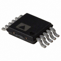
AD8271ARMZ-R7 Analog Devices Inc, AD8271ARMZ-R7 Datasheet - Page 16

AD8271ARMZ-R7
Manufacturer Part Number
AD8271ARMZ-R7
Description
High BW, G = 0.5, 1, 2, 3
Manufacturer
Analog Devices Inc
Datasheet
1.AD8271ARMZ-R7.pdf
(20 pages)
Specifications of AD8271ARMZ-R7
Design Resources
High Speed Instrumentation Amplifier Using AD8271 and ADA4627-1 (CN0122)
Amplifier Type
Programmable Gain
Number Of Circuits
1
Output Type
Rail-to-Rail
Slew Rate
30 V/µs
Gain Bandwidth Product
15MHz
Current - Input Bias
500nA
Voltage - Input Offset
300µV
Current - Supply
2.3mA
Current - Output / Channel
100mA
Voltage - Supply, Single/dual (±)
5 V ~ 36 V, ±2.5 V ~ 18 V
Operating Temperature
-40°C ~ 85°C
Mounting Type
Surface Mount
Package / Case
10-MSOP, Micro10™, 10-uMAX, 10-uSOP
Lead Free Status / RoHS Status
Lead free / RoHS Compliant
-3db Bandwidth
-
Lead Free Status / RoHS Status
Lead free / RoHS Compliant
Other names
AD8271ARMZ-R7TR
Available stocks
Company
Part Number
Manufacturer
Quantity
Price
Company:
Part Number:
AD8271ARMZ-R7
Manufacturer:
MICREL
Quantity:
4 379
AD8271
APPLICATIONS INFORMATION
The resistors and connections provided on the AD8271 offer
abundant versatility through the variety of configurations that
are possible.
DIFFERENCE AMPLIFIER CONFIGURATIONS
The AD8271 can be placed in difference amplifier configurations
with gains of ½, 1, and 2. Figure 45 through Figure 47 show
sample difference amplifier configurations referenced to ground.
Table 8. Pin Connections for Difference Amplifier Configurations
Gain and Reference
Gain of ½, Referenced to Ground
Gain of ½, Referenced to Midsupply
Gain of 1, Referenced to Ground
Gain of 1, Referenced to Midsupply
Gain of 2, Referenced to Ground
Gain of 2, Referenced to Midsupply
GND
GND
+IN
+IN
+IN
NC
GND
Figure 45. Gain = ½ Difference Amplifier, Referenced to Ground
Figure 46. Gain = 1 Difference Amplifier, Referenced to Ground
Figure 47. Gain = 2 Difference Amplifier, Referenced to Ground
P1
P2
P3
P4
P1
P2
P3
P4
P1
P2
P3
P4
1
2
3
4
1
2
3
4
1
2
3
4
10kΩ
10kΩ
20kΩ
20kΩ
10kΩ
10kΩ
20kΩ
20kΩ
10kΩ
10kΩ
20kΩ
20kΩ
AD8271
AD8271
AD8271
10kΩ
10kΩ
10kΩ
10kΩ
10kΩ
10kΩ
10kΩ
10kΩ
10kΩ
10
9
8
7
10
9
8
7
10
N3
N2
N1
OUT
9
8
7
N3
N2
N1
OUT
N3
N2
N1
OUT
OUT
OUT
–IN
–IN
NC
OUT
–IN
OUT
=
=
=
+IN
–IN
Pin 1
(P1)
+IN
+IN
+IN
+IN
+IN
+IN
+IN
–IN
+IN
–IN
10kΩ
10kΩ
10kΩ
10kΩ
5kΩ
5kΩ
GND
GND
GND
5kΩ
10kΩ
10kΩ
5kΩ
10kΩ
10kΩ
Pin 2
(P2)
GND
−V
NC
NC
+IN
+IN
S
Rev. 0 | Page 16 of 20
Pin 3
(P3)
GND
+V
GND
−V
GND
−V
S
S
S
The AD8271 can also be referred to a combination of reference
voltages. For example, the reference can be set at 2.5 V, using
just 5 V and GND. Some of the possible configurations are
shown in Figure 48 through Figure 50. Note that the output
is not internally tied to a feedback path, so any of the 10 kΩ
resistors on the inverting input can be used in the feedback
network. This flexibility allows for more efficient board lay-
out options.
+V
–V
+V
–V
–V
+V
+IN
+IN
+IN
NC
S
S
S
S
S
S
Figure 48. Gain = ½ Difference Amplifier, Referenced to Midsupply
Figure 49. Gain = 1 Difference Amplifier, Referenced to Midsupply
Figure 50. Gain = 2 Difference Amplifier, Referenced to Midsupply
P1
P2
P3
P4
P1
P2
P3
P4
P1
P2
P3
P4
Configuration
1
2
3
4
1
2
3
4
Pin 4
(P4)
GND
+V
GND
+V
GND
+V
1
2
3
4
10kΩ
10kΩ
20kΩ
20kΩ
10kΩ
10kΩ
20kΩ
20kΩ
S
S
S
10kΩ
10kΩ
20kΩ
20kΩ
AD8271
AD8271
AD8271
10kΩ
10kΩ
10kΩ
10kΩ
10kΩ
10kΩ
Pin 8
(N1)
OUT
OUT
OUT
OUT
OUT
OUT
10kΩ
10kΩ
10kΩ
10
10
9
8
7
9
8
7
10
N3
N2
N1
OUT
9
8
7
N3
N2
N1
OUT
N3
N2
N1
OUT
–IN
OUT
OUT
+IN
–IN
NC
OUT
Pin 9
(N2)
OUT
OUT
NC
NC
−IN
−IN
=
=
=
–IN
+IN
+IN
–IN
–IN
+IN
10kΩ
10kΩ
10kΩ
10kΩ
5kΩ
5kΩ
+V
+V
+V
S
S
S
2
+ –V
+ –V
2
+ –V
2
10kΩ
10kΩ
Pin 10
(N3)
−IN
−IN
−IN
−IN
−IN
−IN
5kΩ
10kΩ
S
10kΩ
S
S
5kΩ


