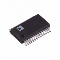
AD9214BRS-65 Analog Devices Inc, AD9214BRS-65 Datasheet - Page 5

AD9214BRS-65
Manufacturer Part Number
AD9214BRS-65
Description
A/D Converter (A-D) IC
Manufacturer
Analog Devices Inc
Datasheet
1.AD9214BRSZ-RL65.pdf
(20 pages)
Specifications of AD9214BRS-65
No. Of Bits
10 Bit
Mounting Type
Surface Mount
No. Of Channels
1
Interface Type
Parallel
Package / Case
28-SSOP
Rohs Status
RoHS non-compliant
Number Of Bits
10
Sampling Rate (per Second)
65M
Data Interface
Parallel
Number Of Converters
1
Power Dissipation (max)
220mW
Voltage Supply Source
Analog and Digital
Operating Temperature
-40°C ~ 85°C
Lead Free Status / RoHS Status
Available stocks
Company
Part Number
Manufacturer
Quantity
Price
Company:
Part Number:
AD9214BRS-65
Manufacturer:
MAXIM
Quantity:
774
Part Number:
AD9214BRS-65
Manufacturer:
ADI/亚德诺
Quantity:
20 000
ABSOLUTE MAXIMUM RATINGS
Electrical
Environmental
NOTES
1
2
Model
AD9214BRS-65
AD9214BRS-80
AD9214BRS-105
AD9214-65PCB
AD9214-105PCB
CAUTION
ESD (electrostatic discharge) sensitive device. Electrostatic charges as high as 4000 V readily
accumulate on the human body and test equipment and can discharge without detection. Although
the AD9214 features proprietary ESD protection circuitry, permanent damage may occur on
devices subjected to high-energy electrostatic discharges. Therefore, proper ESD precautions are
recommended to avoid performance degradation or loss of functionality.
Absolute maximum ratings are limiting values to be applied individually, and
beyond which the serviceability of the circuit may be impaired. Functional
operability is not necessarily implied. Exposure to absolute maximum rating condi-
tions for an extended period of time may affect device reliability.
Typical thermal impedances (package = 28 SSOP); θ
measurements were taken on a 6-layer board in still air with a solid
ground plane.
AV
DrV
Analog Input Voltage . . . . . . . . . . . –0.5 V to AV
Analog Input Current . . . . . . . . . . . . . . . . . . . . . . . 0.4 mA
Digital Input Voltage . . . . . . . . . . . –0.5 V to AV
Digital Output Current . . . . . . . . . . . . . . . . . . 20 mA max
REF Input Voltage . . . . . . . . . . . . . –0.5 V to AV
Operating Temperature Range (Ambient)
Maximum Junction Temperature . . . . . . . . . . . . . . . 150°C
Lead Temperature (Soldering, 10 sec) . . . . . . . . . . . 150°C
Storage Temperature Range (Ambient) . . . –65°C to +150°C
DD
. . . . . . . . . . . . . . . . . . . . . . . . . . . . . . . –40°C to +125°C
DD
Voltage . . . . . . . . . . . . . . . . . . . . . . . . . . . . . 4 V max
Voltage . . . . . . . . . . . . . . . . . . . . . . . . . . . . 4 V max
2
Temperature Range
–40°C to +85°C (Ambient)
–40°C to +85°C (Ambient)
–40°C to +85°C (Ambient)
25°C
25°C
1
JA
= 49°C/W. These
DD
DD
DD
+ 0.5 V
+ 0.5 V
+ 0.5 V
ORDERING GUIDE
Package Description
28-Lead Shrink Small Outline Package
28-Lead Shrink Small Outline Package
28-Lead Shrink Small Outline Package
Evaluation Board with AD9214-65
Evaluation Board with AD9214-105
EXPLANATION OF TEST LEVELS
I
II 100% production tested at 25°C and guaranteed by design
III Sample Tested Only
IV Parameter is guaranteed by design and characterization
V Parameter is a typical value only.
VI 100% production tested at 25°C and guaranteed by design
100% production tested.
and characterization at specified temperatures.
testing.
and characterization for industrial temperature range.
WARNING!
ESD SENSITIVE DEVICE
Package Option
RS-28
RS-28
RS-28
AD9214


