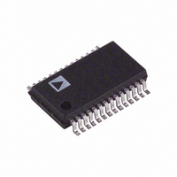
AD9223ARSZ Analog Devices Inc, AD9223ARSZ Datasheet - Page 13

AD9223ARSZ
Manufacturer Part Number
AD9223ARSZ
Description
12-Bit, 1.5/3.0/10 MSPS ADC
Manufacturer
Analog Devices Inc
Specifications of AD9223ARSZ
Number Of Bits
12
Sampling Rate (per Second)
3M
Data Interface
Parallel
Number Of Converters
7
Power Dissipation (max)
130mW
Voltage Supply Source
Single Supply
Operating Temperature
-40°C ~ 85°C
Mounting Type
Surface Mount
Package / Case
28-SSOP (0.200", 5.30mm Width)
Number Of Elements
1
Resolution
12Bit
Architecture
Pipelined
Sample Rate
3MSPS
Input Polarity
Unipolar
Input Type
Voltage
Rated Input Volt
±1/±2.5V
Differential Input
Yes
Power Supply Requirement
Analog and Digital
Single Supply Voltage (typ)
5V
Single Supply Voltage (min)
4.75V
Single Supply Voltage (max)
5.25V
Dual Supply Voltage (typ)
Not RequiredV
Dual Supply Voltage (min)
Not RequiredV
Dual Supply Voltage (max)
Not RequiredV
Power Dissipation
130mW
Differential Linearity Error
±0.75LSB
Integral Nonlinearity Error
±1.25LSB
Operating Temp Range
-40C to 85C
Operating Temperature Classification
Industrial
Mounting
Surface Mount
Pin Count
28
Package Type
SSOP
Lead Free Status / RoHS Status
Lead free / RoHS Compliant
For Use With
AD9223-EB - BOARD EVAL FOR AD9223
Lead Free Status / Rohs Status
Compliant
Available stocks
Company
Part Number
Manufacturer
Quantity
Price
Part Number:
AD9223ARSZ
Manufacturer:
ADI/亚德诺
Quantity:
20 000
Input
Connection
Single-Ended
Single-Ended
Differential
(via Transformer)
*VINA and VINB can be interchanged if signal inversion is required.
REV. E
Coupling Span (V) VINA*
DC
AC
AC
Input
2
2 × VREF 0 to
5
2 × VREF 2.5 – VREF
2 or
2 × VREF 0 to 2 × VREF
5
2 × VREF 2.5 – VREF
2
2 × VREF 2.5 – VREF/2
5
Table I. Analog Input Configuration Summary
0 to 2
2 × VREF
0 to 5
to
2.5 + VREF
0 to 1 or
0 to 5
to
2.5 + VREF
2 to 3
to
2.5 + VREF/2
1.75 to 3.25
Input Range (V)
VINB*
1
VREF
2.5
2.5
1 or VREF
2.5
2.5
3 to 2
2.5 + VREF/2 19
to
2.5 – VREF/2
3.25 to 1.75
–13–
Figure
No.
13, 14
13, 14
13, 14
24
15
15
16
19
19
Comments
Best for stepped input response applica-
tions, suboptimum THD, and noise
performance. Requires ± 5 V op amp.
Same as above but with improved noise
performance due to increase in dynamic
range. Headroom/settling time require-
ments of ± 5 V op amp should be evaluated.
Optimum noise performance, excellent
THD performance. Requires op amp with
VCC > 5 V due to headroom issue.
Optimum THD performance with VREF =
1. Noise to performance improves while
THD performance degrades as VREF
(i.e., 5 V) for many op amps.
Suboptimum ac performance due to input
common-mode level not biased at optimum
midsupply level (i.e., 2.5 V).
Optimum noise performance, excellent THD
performance, ability to use ± 5 V op amp.
Flexible input range, optimum THD
performance with VREF = 1. Noise
performance improves while THD perfor-
mance degrades as VREF increases to 2.5 V.
Ability to use +5 V or ± 5 V op amp.
Optimum full-scale THD and SFDR
performance well beyond the A/D’s Nyquist
frequency. Preferred mode for under-
sampling applications.
Same as 2 V to 3 V input range with the
exception that full-scale THD and SFDR
performance can be traded off for better
noise performance. Refer to discussion in AC
Coupling and Interface Issue section and
Simple AC Interface section.
Optimum Noise performance. Also, the
optimum THD and SFDR performance for
“less than” full-scale signals (i.e., –6 dBFS).
Refer to discussion in AC Coupling and
Interface Issue section and Simple AC
Interface section.
increases to 2.5 V. Single-supply operation
AD9221/AD9223/AD9220


