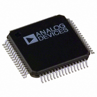
AD9238BST-20 Analog Devices Inc, AD9238BST-20 Datasheet - Page 6

AD9238BST-20
Manufacturer Part Number
AD9238BST-20
Description
IC,A/D CONVERTER,DUAL,12-BIT,CMOS,QFP,64PIN
Manufacturer
Analog Devices Inc
Datasheet
1.AD9238BSTZ-40.pdf
(48 pages)
Specifications of AD9238BST-20
Rohs Compliant
NO
Rohs Status
RoHS non-compliant
Number Of Bits
12
Sampling Rate (per Second)
20M
Data Interface
Parallel
Number Of Converters
2
Power Dissipation (max)
180mW
Voltage Supply Source
Single Supply
Operating Temperature
-40°C ~ 85°C
Mounting Type
Surface Mount
Package / Case
64-LQFP
Lead Free Status / RoHS Status
Available stocks
Company
Part Number
Manufacturer
Quantity
Price
Company:
Part Number:
AD9238BST-20
Manufacturer:
ADI
Quantity:
300
Company:
Part Number:
AD9238BST-20
Manufacturer:
Analog Devices Inc
Quantity:
10 000
Part Number:
AD9238BST-20
Manufacturer:
ADI/亚德诺
Quantity:
20 000
AD9238
DIGITAL SPECIFICATIONS
AVDD = 3 V, DRVDD = 2.5 V, maximum sample rate, CLK_A = CLK_B; A
T
Table 3.
Parameter
LOGIC INPUTS
LOGIC OUTPUTS
1
SWITCHING SPECIFICATIONS
AVDD = 3 V, DRVDD = 2.5 V, maximum sample rate, CLK_A = CLK_B; A
T
Table 4.
Parameter
SWITCHING PERFORMANCE
DATA OUTPUT PARAMETER
OUT-OF-RANGE RECOVERY TIME
1
2
3
Output voltage levels measured with capacitive load only on each output.
The AD9238-65 model has a duty cycle stabilizer circuit that, when enabled, corrects for a wide range of duty cycles (see Figure 24).
Output delay is measured from clock 50% transition to data 50% transition, with a 5 pF load on each output.
Wake-up time is dependent on the value of the decoupling capacitors; typical values shown with 0.1 μF and 10 μF capacitors on REFT and REFB.
MIN
MIN
High Level Input Voltage
Low Level Input Voltage
High Level Input Current
Low Level Input Current
Input Capacitance
High Level Output Voltage
Low Level Output Voltage
Maximum Conversion Rate
Minimum Conversion Rate
CLK Period
CLK Pulse-Width High
CLK Pulse-Width Low
Output Delay
Pipeline Delay (Latency)
Aperture Delay (t
Aperture Uncertainty (t
Wake-Up Time
to T
to T
ANALOG
CLOCK
INPUT
MAX
MAX
DATA
OUT
, DCS enabled, unless otherwise noted.
, DCS enabled, unless otherwise noted.
2
1
3
(t
PD
A
)
)
N–9
1
1
N–1
J
)
Temp
Full
Full
Full
Full
Full
Full
Full
N–8
N
Temp
Full
Full
Full
Full
Full
Full
Full
Full
Full
Full
Full
Test
Level
IV
IV
IV
IV
IV
IV
IV
N–7
N+1
Test
Level
VI
V
V
V
V
VI
V
V
V
V
V
Min
2.0
−10
−10
DRVDD −
0.05
AD9238BST/BCP-20
N–6
N+2
Min
20
50.0
15.0
15.0
2
AD9238BST/BCP-20
Figure 2. Timing Diagram
Rev. C | Page 6 of 48
N–5
Typ
2
Typ
3.5
7
1.0
0.5
2.5
2
N+3
Max
0.8
+10
+10
0.05
Max
1
6
N–4
IN
IN
N+4
= −0.5 dBFS differential input, 1.0 V internal reference,
= −0.5 dBFS differential input, 1.0 V internal reference,
Min
2.0
−10
−10
DRVDD −
0.05
AD9238BST/BCP-40
Min
40
25.0
8.8
8.8
2
AD9238BST/BCP-40
N–3
N+5
Typ
3.5
7
1.0
0.5
2.5
2
Typ
2
N–2
N+6
Max
1
6
Max
0.8
+10
+10
0.05
N–1
N+7
Min
2.0
−10
−10
DRVDD −
0.05
Min
65
15.4
6.2
6.2
2
AD9238BST/BCP-65
AD9238BST/BCP-65
N
Typ
3.5
7
1.0
0.5
2.5
2
t
PD
N+8
=
MIN 2.0ns,
MAX 6.0ns
Typ
2
Max
1
6
Max
0.8
+10
+10
0.05
Unit
MSPS
MSPS
ns
ns
ns
ns
Cycles
ns
ps rms
ms
Cycles
Unit
V
V
μA
μA
pF
V
V


