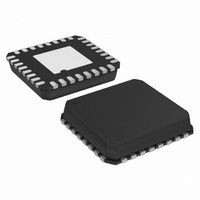
AD9245BCPZ-65 Analog Devices Inc, AD9245BCPZ-65 Datasheet - Page 10

AD9245BCPZ-65
Manufacturer Part Number
AD9245BCPZ-65
Description
IC,A/D CONVERTER,SINGLE,14-BIT,CMOS,LLCC,32PIN
Manufacturer
Analog Devices Inc
Datasheet
1.AD9245BCPZ-80.pdf
(32 pages)
Specifications of AD9245BCPZ-65
Number Of Bits
14
Sampling Rate (per Second)
65M
Data Interface
Parallel
Number Of Converters
3
Power Dissipation (max)
300mW
Voltage Supply Source
Single Supply
Operating Temperature
-40°C ~ 85°C
Mounting Type
Surface Mount
Package / Case
32-VFQFN, CSP Exposed Pad
Lead Free Status / RoHS Status
Lead free / RoHS Compliant
For Use With
AD9245BCP-80EBZ - BOARD EVAL FOR AD9245BCP-80AD9245BCP-40EBZ - BOARD EVAL FOR AD9245BCP-40AD9245BCP-20EBZ - BOARD EVAL FOR AD9245BCP-20
Lead Free Status / RoHS Status
Lead free / RoHS Compliant
AD9245
TERMINOLOGY
Analog Bandwidth (Full Power Bandwidth)
The analog input frequency at which the spectral power of the
fundamental frequency (as determined by the FFT analysis) is
reduced by 3 dB.
Aperture Delay (t
The delay between the 50% point of the rising edge of the clock
and the instant at which the analog input is sampled.
Aperture Uncertainty (Jitter, t
The sample-to-sample variation in aperture delay.
Integral Nonlinearity (INL)
The deviation of each individual code from a line drawn from
negative full scale through positive full scale. The point used as
negative full scale occurs ½ LSB before the first code transition.
Positive full scale is defined as a level 1½ LSB beyond the last
code transition. The deviation is measured from the middle of
each particular code to the true straight line.
Differential Nonlinearity (DNL, No Missing Codes)
An ideal ADC exhibits code transitions that are exactly 1 LSB
apart. DNL is the deviation from this ideal value. Guaranteed
no missing codes to 14-bit resolution indicates that all 16,384
codes must be present over all operating ranges.
Offset Error
The major carry transition should occur for an analog value
½ LSB below VIN+ = VIN–. Offset error is defined as the
deviation of the actual transition from that point.
Gain Error
The first code transition should occur at an analog value ½ LSB
above negative full scale. The last transition should occur at an
analog value 1½ LSB below the positive full scale. Gain error is
the deviation of the actual difference between first and last code
transitions and the ideal difference between first and last code
transitions.
Temperature Drift
The temperature drift for offset error and gain error specifies
the maximum change from the initial (25°C) value to the value
at T
Power Supply Rejection Ratio
The change in full scale from the value with the supply at the
minimum limit to the value with the supply at its maximum limit.
Total Harmonic Distortion (THD)
The ratio of the rms input signal amplitude to the rms value of
the sum of the first six harmonic components.
MIN
or T
MAX
.
A
)
J
)
1
Rev. D | Page 10 of 32
Signal-to-Noise and Distortion (SINAD)
The ratio of the rms input signal amplitude to the rms value of
the sum of all other spectral components below the Nyquist
frequency, including harmonics but excluding dc.
Effective Number of Bits (ENOB)
The effective number of bits for a sine wave input at a given
input frequency can be calculated directly from its measured
SINAD using the following formula:
Signal-to-Noise Ratio (SNR)
The ratio of the rms input signal amplitude to the rms value of
the sum of all other spectral components below the Nyquist
frequency, excluding the first six harmonics and dc.
Spurious-Free Dynamic Range (SFDR)
The difference in dB between the rms input signal amplitude
and the peak spurious signal. The peak spurious component
may or may not be a harmonic.
Two-Tone SFDR
The ratio of the rms value of either input tone to the rms value
of the peak spurious component. The peak spurious component
may or may not be an IMD product.
Clock Pulse Width and Duty Cycle
Pulse width high is the minimum amount of time that the clock
pulse should be left in the Logic 1 state to achieve rated
performance. Pulse width low is the minimum time the clock
pulse should be left in the Logic 0 state. At a given clock rate,
these specifications define an acceptable clock duty cycle.
Minimum Conversion Rate
The clock rate at which the SNR of the lowest analog signal
frequency drops by no more than 3 dB below the guaranteed limit.
Maximum Conversion Rate
The clock rate at which parametric testing is performed.
Output Propagation Delay (t
The delay between the clock rising edge and the time when all
bits are within valid logic levels.
Out-of-Range Recovery Time
The time it takes for the ADC to reacquire the analog input
after a transition from 10% above positive full scale to 10%
above negative full scale, or from 10% below negative full scale
to 10% below positive full scale.
1
AC specifications may be reported in dBc (degrades as signal levels are
lowered) or in dBFS (always related back to converter full scale).
ENOB
=
(
SINAD
1
6.02
−
1.76
)
1
PD
)
1
1


