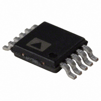
AD9833BRM Analog Devices Inc, AD9833BRM Datasheet - Page 16

AD9833BRM
Manufacturer Part Number
AD9833BRM
Description
10 Bit, 10 Pin DDS
Manufacturer
Analog Devices Inc
Datasheet
1.AD9833BRMZ.pdf
(24 pages)
Specifications of AD9833BRM
Rohs Status
RoHS non-compliant
Resolution (bits)
10 b
Master Fclk
25MHz
Tuning Word Width (bits)
28 b
Voltage - Supply
2.3 V ~ 5.5 V
Operating Temperature
-40°C ~ 105°C
Mounting Type
Surface Mount
Package / Case
10-MSOP, Micro10™, 10-uMAX, 10-uSOP
Resolution
10 Bit
Maximum Input Frequency
25 MHz
Tuning Word Width
28 Bit
Minimum Operating Supply Voltage
2.3 V
Typical Operating Supply Voltage
2.5|3.3|5 V
Maximum Operating Supply Voltage
5.5 V
Minimum Operating Temperature
-40 °C
Maximum Operating Temperature
105 °C
Lead Free Status / RoHS Status
Contains lead / RoHS non-compliant
For Use With
EVAL-AD9833EBZ - BOARD EVAL FOR AD9833
Lead Free Status / RoHS Status
Contains lead / RoHS non-compliant
Available stocks
Company
Part Number
Manufacturer
Quantity
Price
Part Number:
AD9833BRM
Manufacturer:
ADI/亚德诺
Quantity:
20 000
Company:
Part Number:
AD9833BRMZ
Manufacturer:
MICRON
Quantity:
2 154
Company:
Part Number:
AD9833BRMZ
Manufacturer:
ADI
Quantity:
5 000
Part Number:
AD9833BRMZ
Manufacturer:
ADI/亚德诺
Quantity:
20 000
Part Number:
AD9833BRMZ-REEL
Manufacturer:
ADI/亚德诺
Quantity:
20 000
Company:
Part Number:
AD9833BRMZ-REEL7
Manufacturer:
AD
Quantity:
14 592
Part Number:
AD9833BRMZ-REEL7
Manufacturer:
ADI/亚德诺
Quantity:
20 000
AD9833
RESET FUNCTION
The reset function resets appropriate internal registers to 0 to
provide an analog output of midscale. Reset does not reset the
phase, frequency, or control registers. When the AD9833 is
powered up, the part should be reset. To reset the AD9833, set
the reset bit to 1. To take the part out of reset, set the bit to 0. A
signal will appear at the DAC to output eight MCLK cycles after
reset is set to 0.
Table 13. Applying Reset
Reset Bit
0
1
SLEEP FUNCTION
Sections of the AD9833 that are not in use can be powered
down to minimize power consumption. This is done using the
SLEEP function. The parts of the chip that can be powered
down are the internal clock and the DAC. The bits required for
the SLEEP function are outlined in Table 14.
Table 14. Applying the SLEEP Function
SLEEP1 Bit
0
0
1
1
DAC Powered Down
This is useful when the AD9833 is used to output the MSB
of the DAC data only. In this case, the DAC is not required;
therefore, it can be powered down to reduce power
consumption.
Internal Clock Disabled
When the internal clock of the AD9833 is disabled, the DAC
output will remain at its present value because the NCO is no
longer accumulating. New frequency, phase, and control words
can be written to the part when the SLEEP1 control bit is active.
The synchronizing clock is still active, which means that the
selected frequency and phase registers can also be changed
using the control bits. Setting the SLEEP1 bit to 0 enables the
MCLK. Any changes made to the registers while SLEEP1 is
active will be seen at the output after a certain latency.
SLEEP12 Bit
0
1
0
1
Result
No reset applied
Internal registers reset
Result
No power-down
DAC powered down
Internal clock disabled
Both the DAC powered down
and the internal clock disabled
V
OUT
MIN
V
OUT
MAX
Figure 25. Triangle Output
Rev. C | Page 16 of 24
2π
VOUT PIN
The AD9833 offers a variety of outputs from the chip, all of which
are available from the VOUT pin. The choice of outputs is the
MSB of the DAC data, a sinusoidal output, or a triangle output.
The OPBITEN (D5) and mode (D1) bits in the control register
are used to decide which output is available from the AD9833.
MSB of the DAC Data
The MSB of the DAC data can be output from the AD9833. By
setting the OPBITEN (D5) control bit to 1, the MSB of the DAC
data is available at the VOUT pin. This is useful as a coarse
clock source. This square wave can also be divided by two
before being output. The DIV2 (D3) bit in the control register
controls the frequency of this output from the VOUT pin.
Sinusoidal Output
The SIN ROM is used to convert the phase information from
the frequency and phase registers into amplitude information
that results in a sinusoidal signal at the output. To have a sinusoidal
output from the VOUT pin, set the mode (D1) bit to 0 and the
OPBITEN (D5) bit to 0.
Triangle Output
The SIN ROM can be bypassed so that the truncated digital
output from the NCO is sent to the DAC. In this case, the
output is no longer sinusoidal. The DAC will produce a 10-bit
linear triangular function. To have a triangle output from the
VOUT pin, set the mode (D1) bit = 1.
Note that the SLEEP12 bit must be 0 (that is, the DAC is enabled)
when using this pin.
Table 15. Various Outputs from VOUT
OPBITEN Bit
0
0
1
1
1
1
X = don’t care.
4π
Mode Bit
0
1
0
0
1
6π
DIV2 Bit
X
X
0
1
X
1
1
1
VOUT Pin
Sinusoid
Triangle
DAC data MSB/2
DAC data MSB
Reserved


