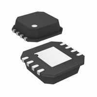
ADA4817-1ACPZ-RL Analog Devices Inc, ADA4817-1ACPZ-RL Datasheet - Page 5

ADA4817-1ACPZ-RL
Manufacturer Part Number
ADA4817-1ACPZ-RL
Description
Hi Speed FET Input Amp
Manufacturer
Analog Devices Inc
Series
FastFET™r
Datasheet
1.ADA4817-1ACPZ-R7.pdf
(24 pages)
Specifications of ADA4817-1ACPZ-RL
Amplifier Type
Voltage Feedback
Number Of Circuits
1
Slew Rate
870 V/µs
Gain Bandwidth Product
410MHz
-3db Bandwidth
1.05GHz
Current - Input Bias
2pA
Voltage - Input Offset
400µV
Current - Supply
19mA
Current - Output / Channel
40mA
Voltage - Supply, Single/dual (±)
5 V ~ 10 V, ±2.5 V ~ 5 V
Operating Temperature
-40°C ~ 105°C
Mounting Type
Surface Mount
Package / Case
8-LFCSP
Lead Free Status / RoHS Status
Lead free / RoHS Compliant
Output Type
-
Lead Free Status / RoHS Status
Lead free / RoHS Compliant
ABSOLUTE MAXIMUM RATINGS
Table 3.
Parameter
Supply Voltage
Power Dissipation
Common-Mode Input Voltage
Differential Input Voltage
Storage Temperature Range
Operating Temperature Range
Lead Temperature
Junction Temperature
Stresses above those listed under Absolute Maximum Ratings
may cause permanent damage to the device. This is a stress
rating only; functional operation of the device at these or any
other conditions above those indicated in the operational
section of this specification is not implied. Exposure to absolute
maximum rating conditions for extended periods may affect
device reliability.
THERMAL RESISTANCE
θ
specified for a device soldered in circuit board for surface-
mount packages.
Table 4.
Package Type
LFCSP_VD (ADA4817-1)
LFSCP_VQ (ADA4817-2)
MAXIMUM SAFE POWER DISSIPATION
The maximum safe power dissipation for the ADA4817-1/
ADA4817-2 are limited by the associated rise in junction
temperature (T
the glass transition temperature), the properties of the plastic
change. Even temporarily exceeding this temperature limit may
change the stresses that the package exerts on the die,
permanently shifting the parametric performance of the
ADA4817. Exceeding a junction temperature of 175°C for an
extended period can result in changes in silicon devices,
potentially causing degradation or loss of functionality.
The power dissipated in the package (P
quiescent power dissipation and the power dissipated in the die
due to the ADA4817-1/ADA4817-2 drive at the output. The
quiescent power is the voltage between the supply pins (V
multiplied by the quiescent current (I
JA
(Soldering, 10 sec)
is specified for the worst-case conditions, that is, θ
J
) on the die. At approximately 150°C (which is
θ
94
64
JA
Rating
10.6 V
See Figure 3
−V
±V
−65°C to +125°C
−40°C to +105°C
300°C
150°C
S
).
S
S
D
) is the sum of the
− 0.5 V to +V
θ
29
14
JC
S
JA
Unit
°C/W
°C/W
+ 0.5 V
is
S
)
Rev. 0 | Page 5 of 24
P
RMS output voltages should be considered. If R
to −V
V
worst-case scenario, when V
In single-supply operation with R
case situation is V
Airflow increases heat dissipation, effectively reducing θ
More metal directly in contact with the package leads and
exposed paddle from metal traces, throughholes, ground,
and power planes also reduces θ
Figure 3 shows the maximum safe power dissipation in the
package vs. the ambient temperature for the exposed paddle
LFCSP_VD (single 94°C/W) and LFCSP_VQ (dual 64°C/W)
package on a JEDEC standard 4-layer board. θ
approximations.
ESD CAUTION
D
Figure 3. Maximum Safe Power Dissipation vs. Ambient Temperature for a
S
= Quiescent Power + (Total Drive Power – Load Power)
× I
P
P
S
OUT
D
, as in single-supply operation, the total drive power is
D
3.5
3.0
2.5
2.0
1.5
1.0
0.5
=
=
. If the rms signal levels are indeterminate, consider the
0
–40
(
(
V
V
S
–30 –20 –10 0
S
×
×
I
I
S
S
OUT
)
) (
ADA4817-2
ADA4817-1
+
+
= V
⎛
⎜
⎜
⎝
V
V
AMBIENT TEMPERATURE (°C)
2
S
R
S
4 /
S
L
/2.
×
10 20 30 40 50 60 70 80 90 100
4-Layer Board
)
ADA4817-1/ADA4817-2
2
V
OUT
R
OUT
L
= V
JA
L
.
⎞
⎟
⎟
⎠
referenced to −V
–
S
/4 for R
V
OUT
R
L
2
L
to midsupply.
JA
L
values are
is referenced
S
, worst-
JA
.
(1)
(2)
(3)


