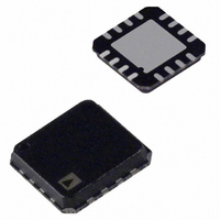
ADA4817-2ACPZ-R7 Analog Devices Inc, ADA4817-2ACPZ-R7 Datasheet - Page 18

ADA4817-2ACPZ-R7
Manufacturer Part Number
ADA4817-2ACPZ-R7
Description
Hi Speed FET Input Amp Dual
Manufacturer
Analog Devices Inc
Series
FastFET™r
Datasheet
1.ADA4817-1ACPZ-R7.pdf
(24 pages)
Specifications of ADA4817-2ACPZ-R7
Amplifier Type
Voltage Feedback
Number Of Circuits
2
Slew Rate
870 V/µs
Gain Bandwidth Product
410MHz
-3db Bandwidth
1.05GHz
Current - Input Bias
2pA
Voltage - Input Offset
400µV
Current - Supply
19mA
Current - Output / Channel
40mA
Voltage - Supply, Single/dual (±)
5 V ~ 10 V, ±2.5 V ~ 5 V
Operating Temperature
-40°C ~ 105°C
Mounting Type
Surface Mount
Package / Case
16-LFCSP
Lead Free Status / RoHS Status
Lead free / RoHS Compliant
Output Type
-
Lead Free Status / RoHS Status
Lead free / RoHS Compliant
Other names
ADA4817-2ACPZ-R7TR
Available stocks
Company
Part Number
Manufacturer
Quantity
Price
Company:
Part Number:
ADA4817-2ACPZ-R7
Manufacturer:
AD
Quantity:
5 271
ADA4817-1/ADA4817-2
APPLICATIONS INFORMATION
LOW DISTORTION PINOUT
The ADA4817-1/ADA4817-2 feature a new low distortion
pinout from Analog Devices. The new pinout provides two
advantages over the traditional pinout. The first advantage is
improved second harmonic distortion performance, which is
accomplished by the physical separation of the noninverting
input pin and the negative power supply pin. The second
advantage is the simplification of the layout due to the dedi-
cated feedback pin and easy routing of the gain set resistor
back to the inverting input pin. This allows a compact layout,
which helps to minimize parasitics and increase stability.
The designer does not need to use the dedicated feedback pin to
provide feedback for the ADA4817-1/ADA4817-2. The output
pin of the ADA4817-1/ADA4817-2 can still be used to provide
feedback to the inverting input of the ADA4817-1/ADA4817-2.
WIDEBAND PHOTODIODE PREAMP
The wide bandwidth and low noise of the ADA4817-1/
ADA4817-2 make it an ideal choice for transimpedance
amplifiers, such as those used for signal conditioning with
high speed photodiodes. Figure 44 shows an I/V converter
with an electrical model of a photodiode. The basic transfer
function is
where:
I
The parallel combination of R
PHOTO
I
PHOTO
V
is the output current of the photodiode.
OUT
V
=
B
I
1
PHOTO
C
Figure 44. Wideband Photodiode Preamp
+
S
sC
R
F
×
SH
R
R
F
= 10
F
11
Ω
F
and C
C
D
F
sets the signal bandwidth.
C
C
M
M
C
R
F
F
V
OUT
(13)
Rev. 0 | Page 18 of 24
The stable bandwidth attainable with this preamp is a function
of R
capacitance at the amplifier’s summing junction, including the
photodiode capacitance (C
R
loop transmission that can result in peaking and instability.
Adding C
sates for the pole’s effect and reduces the signal bandwidth. It
can be shown that the signal bandwidth obtained with a 45°
phase margin (f
where:
f
R
C
board parasitic.
C
C
The value of C
The frequency response shows less peaking if bigger C
are used.
The preamplifier output noise over frequency is shown in
Figure 45.
CR
F
F
S
M
D
is the feedback resistor.
is the source capacitance including the photodiode and the
and the total capacitance produce a pole in the amplifier’s
is the amplifier crossover frequency.
is the differential capacitance of the amplifier.
F
is the common-mode capacitance of the amplifier.
, the gain bandwidth product of the amplifier, and the total
C
f
(
F
45
)
=
F
=
VEN
Figure 45. Photodiode Voltage Noise Contributions
creates a zero in the loop transmission that compen-
f
C
2
1
R
2
π
S
F
F
π
NOISE
(45)
×
that produces f
+
×
NOISE DUE TO AMPLIFIER
C
R
) is defined by
R
M
F
f
f
f
f
2
F
1
2
3
×
=
=
=
+
×
2 R
2 R
(C
(
C
f
C
CR
F
FREQUENCY (Hz)
f
D
VEN (C
1
S
S
+ C
CR
F
F
) and the amplifier input capacitance.
C
(C
+
F
S
F
C
+ C
+ C
f
F
(45)
CR
M
+ C
1
M
S
+
can be shown to be
+ C
+ C
S
C
+ C
D
M
D
)/C
+ C
M
)
F
+ C
D
)
D
)/C
F
f
3
F
values
(14)
(15)


