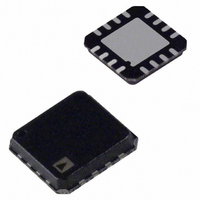
ADA4937-1YCPZ-RL Analog Devices Inc, ADA4937-1YCPZ-RL Datasheet - Page 8

ADA4937-1YCPZ-RL
Manufacturer Part Number
ADA4937-1YCPZ-RL
Description
IC,Differential Amplifier,SINGLE,BIPOLAR,LLCC,16PIN,PLASTIC
Manufacturer
Analog Devices Inc
Type
ADC Driverr
Datasheet
1.ADA4937-1YCPZ-R7.pdf
(28 pages)
Specifications of ADA4937-1YCPZ-RL
Design Resources
Driving AD9233/46/54 ADCs in AC-Coupled Baseband Appls (CN0051)
Applications
Data Acquisition
Mounting Type
Surface Mount
Package / Case
16-LFCSP
Lead Free Status / RoHS Status
Lead free / RoHS Compliant
ADA4937-1/ADA4937-2
PIN CONFIGURATIONS AND FUNCTION DESCRIPTIONS
Table 7. ADA4937-1 Pin Function Descriptions
Pin No.
1
2
3
4
5 to 8
9
10
11
12
13 to 16
EP
NOTES
1. EXPOSED PADDLE. THE EXPOSED PAD IS NOT
ELECTRICALLY CONNECTED TO THE DEVICE. IT IS
TYPICALLY SOLDERED TO GROUND OR A POWER
PLANE ON THE PCB THAT IS THERMALLY CONDUCTIVE.
Mnemonic
−FB
+IN
−IN
+FB
+V
V
+OUT
−OUT
PD
−V
OCM
S
S
Figure 5. ADA4937-1 Pin Configuration
+FB
–FB
+IN
–IN
1
2
3
4
Description
Negative Output for Feedback
Component Connection.
Positive Input Summing Node.
Negative Input Summing Node.
Positive Output for Feedback
Component Connection.
Positive Supply Voltage.
Output Common-Mode Voltage.
Positive Output for Load Connection.
Negative Output for Load Connection.
Power-Down Pin.
Negative Supply Voltage.
Exposed Paddle. The exposed pad is not
electrically connected to the device. It is
typically soldered to ground or a power
plane on the PCB that is thermally
conductive.
ADA4937-1
(Not to Scale)
TOP VIEW
PIN 1
INDICATOR
12 PD
11 –OUT
10 +OUT
9 V
OCM
Rev. C | Page 8 of 28
Table 8. ADA4937-2 Pin Function Descriptions
Pin No.
1
2
3, 4
5
6
7
8
9, 10
11
12
13
14
15, 16
17
18
19
20
21, 22
23
24
EP
NOTES
1. EXPOSED PADDLE. THE EXPOSED PAD IS NOT
ELECTRICALLY CONNECTED TO THE DEVICE. IT IS
TYPICALLY SOLDERED TO GROUND OR A POWER
PLANE ON THE PCB THAT IS THERMALLY CONDUCTIVE.
Mnemonic
−IN1
+FB1
+V
−FB2
+IN2
−IN2
+FB2
+V
V
+OUT2
−OUT2
PD2
−V
V
+OUT1
−OUT1
PD1
−V
−FB1
+IN1
OCM2
OCM1
S1
S2
S2
S1
Figure 6. ADA4937-2 Pin Configuration
+FB1
–FB2
+V
+V
+IN2
–IN1
S1
S1
1
2
3
4
5
6
ADA4937-2
(Not to Scale)
Description
Negative Input Summing Node 1.
Positive Output Feedback Pin 1.
Positive Supply Voltage 1.
Negative Output Feedback Pin 2.
Positive Input Summing Node 2.
Negative Input Summing Node 2.
Positive Output Feedback Pin 2.
Positive Supply Voltage 2.
Output Common-Mode Voltage 2.
Positive Output 2.
Negative Output 2.
Power-Down Pin 2.
Negative Supply Voltage 2.
Output Common-Mode Voltage 1.
Positive Output 1.
Negative Output 1.
Power-Down Pin 1.
Negative Supply Voltage 1.
Negative Output Feedback Pin 1.
Positive Input Summing Node 1.
Exposed Paddle. The exposed pad is
not electrically connected to the
device. It is typically soldered to
ground or a power plane on the PCB
that is thermally conductive.
TOP VIEW
PIN 1
INDICATOR
18
17
16
15
14
13
+OUT1
V
–V
–V
PD2
–OUT2
OCM1
S2
S2


