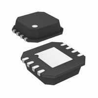
ADA4941-1YCPZ-R7 Analog Devices Inc, ADA4941-1YCPZ-R7 Datasheet - Page 20

ADA4941-1YCPZ-R7
Manufacturer Part Number
ADA4941-1YCPZ-R7
Description
Amplifier, Other
Manufacturer
Analog Devices Inc
Type
ADC Driverr
Datasheet
1.ADA4941-1YCPZ-R7.pdf
(24 pages)
Specifications of ADA4941-1YCPZ-R7
Design Resources
Converting a Single-Ended Signal with AD7982 Differential PulSAR ADC (CN0032) Converting a Single-Ended Signal with AD7984 Differential PulSAR ADC (CN0033)
Applications
Data Acquisition
Mounting Type
Surface Mount
Package / Case
8-LFCSP
Lead Free Status / RoHS Status
Lead free / RoHS Compliant
Other names
ADA4941-1YCPZ-R7TR
Available stocks
Company
Part Number
Manufacturer
Quantity
Price
Company:
Part Number:
ADA4941-1YCPZ-R7
Manufacturer:
Intersil
Quantity:
254
ADA4941-1
APPLICATIONS
OVERVIEW
The ADA4941-1 is an adjustable-gain, single-ended-to-differential
voltage amplifier, optimized for driving high resolution ADCs.
Single-ended-to-differential gain is controlled by one feedback
network, comprised of two external resistors: R
USING THE REF PIN
The REF pin sets the output base line in the inverting path and
is used as a reference for the input signal. In most applications,
the REF pin is set to the input signal midswing level, which in
many cases is also midsupply. For bipolar signals and dual
power supplies, REF is generally set to ground. In single-supply
applications, setting REF to the input signal midswing level
provides optimal output dynamic range performance with
minimum differential offset. Note that the REF input only
affects the inverting signal path or VON.
Most applications require a differential output signal with the
same dc common-mode level on each output. It is possible for
the signal measured across VOP and VON to have a common-
mode voltage that is of the desired level but not common to
both outputs. This type of signal is generally avoided because
it does not allow for optimal use of the amplifier’s output
dynamic range.
Defining VIN as the voltage applied to the input pin, the
equations that govern the two signal paths are given in
Equation 21 and Equation 22.
When the REF voltage is set to the midswing level of the input
signal, the two output signals fall directly on top of each other
with minimal offset. Setting the REF voltage elsewhere results
in an offset between the two outputs.
VOP = VIN
VON = −VIN + 2 (REF)
F
and R
G
.
(21)
(22)
Rev. B | Page 20 of 24
The best use of the REF pin can be further illustrated by
considering a single-supply case with a 10 V power supply and
an input signal that varies between 2 V and 7 V. This is a case
where the midswing level of the input signal is not at midsupply
but is at 4.5 V. Setting the REF input at 4.5 V and neglecting
offsets, Equation 21 and Equation 22 are used to calculate the
results. When the input signal is at its midpoint of 4.5 V,
OUT+ is at 4.5 V, as is VON. This can be considered as a base
line state where the differential output voltage is 0. When the
input increases to 7 V, VOP tracks the input to 7 V, and VON
decreases to 2 V. This can be viewed as a positive peak signal
where the differential output voltage equals 5 V. When the input
signal decreases to 2 V, VOP again tracks to 2 V, and VON
increases to 7 V. This can be viewed as a negative peak signal
where the differential output voltage equals −5 V. The resulting
differential output voltage is 10 V p-p.
The previous discussion reveals how the single-ended-to-
differential gain of 2 is achieved.
INTERNAL FEEDBACK NETWORK POWER
DISSIPATION
While traditional op amps do not have on-chip feedback
elements, the ADA4941-1 contains two on-chip, 1 kΩ resistors
that comprise an internal feedback loop. The power dissipated
in these resistors must be included in the overall power dissipation
calculations for the device. Under certain circumstances, the
power dissipated in these resistors could be comparable to the
device’s quiescent dissipation. For example, on ±5 V supplies
with the REF pin tied to ground and OUT− at +4 VDC, each
1 kΩ resistor carries 4 mA and dissipates 16 mW for a total of
32 mW. This is comparable to the quiescent power and must
therefore be included in the overall device power dissipation
calculations. For ac signals, rms analysis is required.
DISABLE FEATURE
The ADA4941-1 includes a disable feature that can be asserted
to minimize power consumption in a device that is not needed
at a particular time. When asserted, the disable feature does not
place the device output in a high impedance or tristate condition.
The disable feature is active high. See the Specifications tables
for the high and low level voltage specifications.


