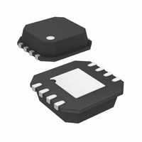
ADA4941-1YCPZ-RL Analog Devices Inc, ADA4941-1YCPZ-RL Datasheet - Page 10

ADA4941-1YCPZ-RL
Manufacturer Part Number
ADA4941-1YCPZ-RL
Description
Amplifier, Other
Manufacturer
Analog Devices Inc
Type
ADC Driverr
Datasheet
1.ADA4941-1YCPZ-R7.pdf
(24 pages)
Specifications of ADA4941-1YCPZ-RL
Design Resources
Converting a Single-Ended Signal with AD7982 Differential PulSAR ADC (CN0032) Converting a Single-Ended Signal with AD7984 Differential PulSAR ADC (CN0033)
Applications
Data Acquisition
Mounting Type
Surface Mount
Package / Case
8-LFCSP
Number Of Channels
1
Number Of Elements
2
Power Supply Requirement
Single
Common Mode Rejection Ratio
84dB
Voltage Gain Db
6.06dB
Unity Gain Bandwidth Product (typ)
31MHz
Input Resistance
24@5VMohm
Input Offset Voltage
0.4@5VmV
Input Bias Current
4.5@5VnA
Single Supply Voltage (typ)
3/5/9V
Dual Supply Voltage (typ)
Not RequiredV
Power Supply Rejection Ratio
87dB
Rail/rail I/o Type
Rail to Rail Output
Single Supply Voltage (min)
2.7V
Single Supply Voltage (max)
12V
Dual Supply Voltage (min)
Not RequiredV
Dual Supply Voltage (max)
Not RequiredV
Operating Temp Range
-40C to 125C
Operating Temperature Classification
Automotive
Mounting
Surface Mount
Pin Count
8
Package Type
LFCSP EP
Lead Free Status / RoHS Status
Lead free / RoHS Compliant
Lead Free Status / RoHS Status
Lead free / RoHS Compliant
ADA4941-1
Figure 17. Distortion vs. Output Amplitude for Various Supplies (G = +2)
Figure 19. Distortion vs. Frequency at Various Output Amplitudes
–100
–105
–120
–125
–130
–135
–140
–100
–105
–120
–125
–130
–135
–140
–110
–115
–110
–115
–105
–115
–125
–135
–60
–65
–70
–75
–80
–85
–90
–95
–60
–65
–70
–75
–80
–85
–90
–95
–65
–75
–85
–95
0.1
0.1
Figure 18. Distortion vs. Frequency for Various Supplies
0
V
VREF = MIDSUPPLY
HD3
HD3
HD2
O, dm
HD2
HD3
2
HD3
= 2V p-p
V
HD2
S
4
= +3V
1
1
HD2
OUTPUT AMPLITUDE (V p-p)
HD2
HD2
6
HD3
FREQUENCY (kHz)
FREQUENCY (kHz)
V
S
HD3
8
= +5V
10
10
10
f
= 10kHz
12
V
O
14
HD3
= 6V p-p
V
100
100
S
= ±5V
HD2
V
16
O
V
V
V
= 2V p-p
S
S
S
= +3V
= +5V
= ±5V
18
1000
1000
20
Rev. B | Page 10 of 24
Figure 22. Small Signal Transient Response for Various Capacitive Loads
Figure 20. Distortion vs. Output Amplitude for Various Supplies (G = −2)
–100
–110
–120
–130
–140
–105
–125
–135
–145
–0.04
–0.08
–0.12
–115
–70
–80
–90
–65
–75
–85
–95
0.12
0.08
0.04
0.1
0
0
Figure 21. Distortion vs. Frequency for Various Gains
V
VREF = MIDSUPPLY
O, dm
HD3
HD3
2
V
= 2V p-p
S
HD3
= +3V
HD2
4
1
HD2
OUTPUT AMPLITUDE (V p-p)
6
HD3
FREQUENCY (kHz)
HD3
8
C
C
L
L
= 0pF
= 20pF
10
10
HD2
V
S
HD3
= +5V
12
DIFFERENTIAL G = –2
f
= 10kHz
14
V
100
OUT
16
= 200mV p-p
V
S
= ±5V
50ns/DIV
G = –2
G = +2
G = +4
18
1000
2
0


