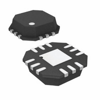
ADCMP605BCPZ-WP Analog Devices Inc, ADCMP605BCPZ-WP Datasheet

ADCMP605BCPZ-WP
Specifications of ADCMP605BCPZ-WP
Available stocks
Related parts for ADCMP605BCPZ-WP
ADCMP605BCPZ-WP Summary of contents
Page 1
FEATURES Fully specified rail to rail 2 5.5 V CCI Input common-mode voltage from −0 Low glitch LVDS-compatible output stage 1.6 ns propagation delay 2.5 V Shutdown pin Single-pin ...
Page 2
ADCMP604/ADCMP605 TABLE OF CONTENTS Features .............................................................................................. 1 Applications....................................................................................... 1 Functional Block Diagram .............................................................. 1 General Description ......................................................................... 1 Revision History ............................................................................... 2 Specifications..................................................................................... 3 Electrical Characteristics............................................................. 3 Timing Information ......................................................................... 5 Absolute Maximum Ratings............................................................ 6 Thermal Resistance ...................................................................... 6 ESD ...
Page 3
SPECIFICATIONS ELECTRICAL CHARACTERISTICS 2 −40°C to +125°C, typical at T CCI CCO A Table 1. Parameter DC INPUT CHARACTERISTICS Voltage Range Common-Mode Range Differential Voltage Offset Voltage Bias Current Offset Current Capacitance Resistance, ...
Page 4
ADCMP604/ADCMP605 Parameter 1 AC PERFORMANCE Rise Time/Fall Time Propagation Delay Propagation Delay Skew—Rising to Falling Transition Propagation Delay Skew— Overdrive Dispersion Common-Mode Dispersion Input Bandwidth Minimum Pulse Width POWER SUPPLY Input Supply Voltage Range Output Supply Voltage Range ...
Page 5
TIMING INFORMATION Figure 2 illustrates the ADCMP604/ADCMP605 latch timing relationships. Table 2 provides definitions of the terms shown in Figure 2. LATCH ENABLE DIFFERENTIAL INPUT VOLTAGE Q OUTPUT Q OUTPUT Table 2. Timing Descriptions Symbol Timing t Input-to-Output High Delay ...
Page 6
ADCMP604/ADCMP605 ABSOLUTE MAXIMUM RATINGS Table 3. Parameter Supply Voltages Input Supply Voltage (V to GND) CCI Output Supply Voltage (V to GND) CCO Positive Supply Differential (V − V CCI CCO Input Voltages Input Voltage Differential Input Voltage Maximum Input/Output ...
Page 7
PIN CONFIGURATION AND FUNCTION DESCRIPTIONS Table 5. ADCMP604 Pin Function Descriptions (6-Lead SC70) Pin No. Mnemonic Description 1 Q Noninverting Output logic high if the analog voltage at the noninverting input, V analog voltage at the inverting ...
Page 8
ADCMP604/ADCMP605 TYPICAL PERFORMANCE CHARACTERISTICS 2 25°C, unless otherwise noted. CCI CCO A 800 600 400 V = 2.5V CC 200 0 –200 –400 –600 –800 – LE/HYS PIN (V) ...
Page 9
HYS PIN CURRENT (µA) Figure 11. Hysteresis vs. HYS Pin Current 3.5 3.0 2.5 2.0 PROPAGATION DELAY 1.5 1 ...
Page 10
ADCMP604/ADCMP605 APPLICATION INFORMATION POWER/GROUND LAYOUT AND BYPASSING The ADCMP604/ADCMP605 comparators are very high speed devices. Despite the low noise output stage essential to use proper high speed design techniques to achieve the specified performance. Because comparators are uncompensated ...
Page 11
COMPARATOR PROPAGATION DELAY DISPERSION The ADCMP604/ADCMP605 comparators are designed to reduce propagation delay dispersion over a wide input overdrive range − Propagation delay dispersion is the CCI variation in propagation delay that results ...
Page 12
ADCMP604/ADCMP605 The hysteresis control pin appears as a 1.25 V bias voltage seen through a series resistance of 70 kΩ ± 20% throughout the hysteresis control range. The advantages of applying hysteresis in this manner are improved accuracy, improved stability, ...
Page 13
TYPICAL APPLICATION CIRCUITS 2. 0.1µF INPUT 2kΩ ADCMP604 2kΩ 0.1µF Figure 21. Self-Biased, 50% Slicer 2.5V TO 3.3V ADCMP604 LVDS 100Ω Figure 22. LVDS to Repeater 2. ADCMP605 DIGITAL 74VHC INPUT 1G07 150kΩ CONTROL VOLTAGE 0V ...
Page 14
... ORDERING GUIDE Model Temperature Range 1 ADCMP604BKSZ-R2 −40°C to +125°C 1 ADCMP604BKSZ-REEL7 −40°C to +125°C ADCMP604BKSZ-RL 1 −40°C to +125°C 1 ADCMP605BCPZ-WP −40°C to +125°C 1 ADCMP605BCPZ-R2 −40°C to +125°C 1 ADCMP605BCPZ-R7 −40°C to +125°C EVAL-ADCMP605BCPZ RoHS Compliant Part. 2.20 2.00 1 ...
Page 15
NOTES Rev Page ADCMP604/ADCMP605 ...
Page 16
ADCMP604/ADCMP605 NOTES ©2006–2007 Analog Devices, Inc. All rights reserved. Trademarks and registered trademarks are the property of their respective owners. D05916-0-8/07(A) T Rev Page ...


