ADG1219BRJZ-REEL7 Analog Devices Inc, ADG1219BRJZ-REEL7 Datasheet
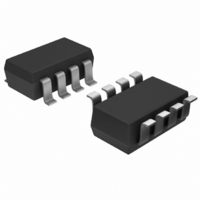
IC,ANALOG SWITCH,SINGLE,SPDT,CMOS,TSSOP,8PIN,PLASTIC

ADG1219BRJZ-REEL7

Manufacturer Part Number
ADG1219BRJZ-REEL7
Description
IC,ANALOG SWITCH,SINGLE,SPDT,CMOS,TSSOP,8PIN,PLASTIC
Manufacturer
Analog Devices Inc
Series
iCMOS®r
Type
Analog Switchr
Datasheet

Specifications of ADG1219BRJZ-REEL7

Function
Switch
Circuit
1 x SPDT
On-state Resistance
270 Ohm
Voltage Supply Source
Single Supply
Voltage - Supply, Single/dual (±)
12 V ~ 15 V
Current - Supply
1µA
Operating Temperature
-40°C ~ 85°C
Mounting Type
Surface Mount
Package / Case
SOT-23-8
Multiplexer Configuration
Single SPDT
Number Of Inputs
1
Number Of Outputs
2
Number Of Channels
1
Analog Switch On Resistance
475@10.8VOhm
Package Type
SOT-23
Power Supply Requirement
Single/Dual
Single Supply Voltage (typ)
12V
Dual Supply Voltage (typ)
±15V
Mounting
Surface Mount
Pin Count
8
Operating Temp Range
-40C to 125C
Operating Temperature Classification
Automotive
Package
8SOT-23
Maximum On Resistance
475@10.8V Ohm
Maximum Propagation Delay Bus To Bus
170@±15V|250@12V ns
Maximum High Level Output Current
30 mA
Maximum Turn-off Time
185@12V ns
Maximum Turn-on Time
150@12V ns
Switch Architecture
SPDT
Power Supply Type
Single|Dual
Lead Free Status / RoHS Status
Lead free / RoHS Compliant
Lead Free Status / RoHS Status
Lead free / RoHS Compliant
Other names
ADG1219BRJZ-REEL7TR

Available stocks

Company
Part Number
Manufacturer
Quantity
Price
Part Number:
ADG1219BRJZ-REEL7
Manufacturer:
Allegro
Quantity:
48 573
FEATURES
<0.5 pC charge injection over full signal range
2.5 pF off capacitance
Low leakage; 0.6 nA maximum @ 85°C
120 Ω on resistance
Fully specified at +12 V, ±15 V
No V
3 V logic-compatible inputs
Rail-to-rail operation
8-lead SOT-23 package
APPLICATIONS
Automatic test equipment
Data acquisition systems
Battery-powered systems
Sample-and-hold systems
Audio/video signal routing
Communication systems
GENERAL DESCRIPTION
The ADG1219 is a monolithic iCMOS® device containing an
SPDT switch. An EN input is used to enable or disable the
device. When disabled, all channels are switched off. When on,
each channel conducts equally well in both directions and has
an input signal range that extends to the supplies. Each switch
exhibits break-before-make switching action.
The iCMOS (industrial CMOS) modular manufacturing
process combines high voltage complementary metal-oxide
semiconductor (CMOS) and bipolar technologies. It enables the
development of a wide range of high performance analog ICs
capable of 33 V operation in a footprint that no other generation
of high voltage parts has been able to achieve. Unlike analog ICs
using conventional CMOS processes, iCMOS components can
tolerate high supply voltages while providing increased perfor-
mance, dramatically lower power consumption, and reduced
package size.
The ultralow capacitance and exceptionally low charge injection
of these multiplexers make them ideal solutions for data acquisi-
tion and sample-and-hold applications, where low glitch and
fast settling are required. Figure 2 shows that there is minimum
Rev. A
Information furnished by Analog Devices is believed to be accurate and reliable. However, no
responsibility is assumed by Analog Devices for its use, nor for any infringements of patents or other
rights of third parties that may result from its use. Specifications subject to change without notice. No
license is granted by implication or otherwise under any patent or patent rights of Analog Devices.
Trademarks and registered trademarks are the property of their respective owners.
L
supply required
Low Capacitance, Low Charge Injection,
±15 V/12 V iCMOS SPDT in SOT-23
One Technology Way, P.O. Box 9106, Norwood, MA 02062-9106, U.S.A.
Tel: 781.329.4700
Fax: 781.461.3113
charge injection over the entire signal range of the device.
iCMOS construction also ensures ultralow power dissipation,
making the parts ideally suited for portable and battery-
powered instruments.
–0.1
–0.2
–0.3
–0.4
–0.5
0.5
0.4
0.3
0.2
0.1
0
–15
T
FUNCTIONAL BLOCK DIAGRAM
A
SWITCHES SHOWN FOR A LOGIC 0 INPUT
= 25ºC
Figure 2. Charge Injection vs. Input Voltage
SA
SB
–10
©2008–2009 Analog Devices, Inc. All rights reserved.
V
V
DD
SS
V
V
= –5V
= +5V
ADG1219
DD
SS
–5
DECODER
INPUT VOLTAGE (V)
IN
= –15V
= +15V
Figure 1.
EN
0
D
5
ADG1219
V
V
DD
SS
www.analog.com
10
= 0V
= +12V
15

Related parts for ADG1219BRJZ-REEL7

ADG1219BRJZ-REEL7 Summary of contents

Page 1

FEATURES <0.5 pC charge injection over full signal range 2.5 pF off capacitance Low leakage; 0.6 nA maximum @ 85°C 120 Ω on resistance Fully specified at +12 V, ± supply required logic-compatible inputs ...

Page 2

ADG1219 TABLE OF CONTENTS Features .............................................................................................. 1 Applications ....................................................................................... 1 Functional Block Diagram .............................................................. 1 General Description ......................................................................... 1 Revision History ............................................................................... 2 Specifications ..................................................................................... 3 Dual Supply ................................................................................... 3 Single Supply ................................................................................. 4 REVISION HISTORY 3/09—Rev Rev. ...

Page 3

SPECIFICATIONS DUAL SUPPLY ± 10 −15 V ± 10%, GND = 0 V, unless otherwise noted Table 1. Parameters ANALOG SWITCH Analog Signal Range On Resistance Resistance Match Between ...

Page 4

ADG1219 Parameters POWER REQUIREMENTS Temperature range for B version is −40°C to +125°C. 2 Guaranteed by design; not subject to production test. SINGLE SUPPLY ± ...

Page 5

Parameters C (Off (Off (On POWER REQUIREMENTS Temperature range for B version is −40°C to +125°C. 2 Guaranteed by design; not subject to production test. ...

Page 6

ADG1219 ABSOLUTE MAXIMUM RATINGS T = 25°C, unless otherwise noted. A Table 3. Parameter Rating GND −0 + GND +0 − ...

Page 7

PIN CONFIGURATION AND FUNCTION DESCRIPTIONS Table 4. Pin Function Descriptions Pin No. Mnemonic Description 1 EN Active High Digital Input. When this pin is low, the device is disabled and all switches are turned off. When this pin is high, ...

Page 8

ADG1219 TYPICAL PERFORMANCE CHARACTERISTICS 200 T = 25°C A 180 V = 13.5V 160 –13.5V SS 140 120 V 100 –18 –15 –12 –9 –6 – SOURCE ...

Page 9

V = 12V 0 1V/10V BIAS 0.4 0.3 0.2 0.1 0 –0.1 –0.2 –0 TEMPERATURE (°C) Figure 10. Leakage Currents as a Function of Temperature Single ...

Page 10

ADG1219 15V DD – –15V 25ºC –20 A –30 –40 –50 –60 –70 –80 –90 –100 –110 10k 100k 1M 10M FREQUENCY (Hz) Figure 16. Crosstalk vs. Frequency 15V ...

Page 11

V = +15V DD – –15V SS NO DECOUPLING CAPS ON V p-p = 0.63V – 25°C A –30 –40 –50 –60 DECOUPLING CAPS ON –70 –80 –90 –100 100k 1M 10M FREQUENCY (Hz) Figure ...

Page 12

ADG1219 TEST CIRCUITS Figure 23. On Resistance I (OFF Figure 24. Off Leakage CONNECT Figure 25. On Leakage ...

Page 13

0.1µF 0.1µ 300Ω 35pF IN V GND IN Figure 30. Switching Times 0.1µF 0.1µ ...

Page 14

ADG1219 TERMINOLOGY I DD The positive supply current The negative supply current The analog voltage on Terminal D and Terminal The ohmic resistance between Terminal D and Terminal S. R ...

Page 15

... OUTLINE DIMENSIONS 1.70 1.60 1.50 PIN 1 INDICATOR 1.30 1.15 0.90 0.15 MAX 0.05 MIN ORDERING GUIDE Model Temperature Range 1 ADG1219BRJZ-R2 −40°C to +125°C 1 ADG1219BRJZ-REEL7 −40°C to +125° RoHS Compliant Part. 3.00 2.90 2. 3.00 2.80 2. 0.65 BSC 1.95 BSC 0.22 MAX 1 ...

Page 16

ADG1219 NOTES ©2008–2009 Analog Devices, Inc. All rights reserved. Trademarks and registered trademarks are the property of their respective owners. D06575-0-3/09(A) Rev Page ...

Related keywords