ADG528ATQ Analog Devices Inc, ADG528ATQ Datasheet
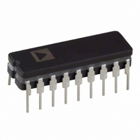
IC,ANALOG MUX,SINGLE,8-CHANNEL,CMOS,DIP,18PIN,CERAMIC

ADG528ATQ

Manufacturer Part Number
ADG528ATQ
Description
IC,ANALOG MUX,SINGLE,8-CHANNEL,CMOS,DIP,18PIN,CERAMIC
Manufacturer
Analog Devices Inc
Datasheet

Specifications of ADG528ATQ

Rohs Status
RoHS non-compliant
Function
Multiplexer
Circuit
1 x 8:1
On-state Resistance
300 Ohm
Voltage Supply Source
Dual Supply
Voltage - Supply, Single/dual (±)
±10.8 V ~ 16.5 V
Current - Supply
20µA
Operating Temperature
-55°C ~ 125°C
Mounting Type
Through Hole
Package / Case
18-CDIP (0.300", 7.62mm)
Lead Free Status / RoHS Status

Available stocks

Company
Part Number
Manufacturer
Quantity
Price
Part Number:
ADG528ATQ
Manufacturer:
NS
Quantity:
780
Part Number:
ADG528ATQ/883
Manufacturer:
AD
Quantity:
550
Part Number:
ADG528ATQ/883B
Manufacturer:
TI
Quantity:
65
GENERAL DESCRIPTION
The ADG528A and ADG529A are CMOS monolithic analog
multiplexers with eight channels and four dual channels, respec-
tively. On-chip latches facilitate microprocessor interfacing. The
ADG528A switches one of eight inputs to a common output,
depending on the state of three binary addresses and an enable
input. The ADG529A switches one of four differential inputs to
a common differential output, depending on the state of two
binary addresses and an enable input. Both devices have TTL
and 5 V CMOS logic-compatible digital inputs.
The ADG528A and ADG529A are designed on an enhanced
LC
V
voltages. The devices can comfortably operate anywhere in the
10.8 V to 16.5 V single- or dual-supply range. These multiplex-
ers also feature high switching and low R
REV. B
Information furnished by Analog Devices is believed to be accurate and
reliable. However, no responsibility is assumed by Analog Devices for its
use, nor for any infringements of patents or other rights of third parties that
may result from its use. No license is granted by implication or otherwise
under any patent or patent rights of Analog Devices. Trademarks and
registered trademarks are the property of their respective owners.
SS
FEATURES
44 V Supply Maximum Rating
V
Single-/Dual-Supply Specifications
Wide Supply Ranges (10.8 V to 16.5 V)
Microprocessor Compatible (100 ns WR Pulse)
Extended Plastic Temperature Range
Low Leakage (20 pA typ)
Low Power Dissipation (28 mW max)
Available in 18-Lead DIP/SOIC and 20-Lead PLCC Packages
Superior Alternative to:
2
to V
MOS process, which gives an increased signal capability of
SS
(–40°C to +85°C)
DG528
DG529
to V
DD
and enables operation over a wide range of supply
DD
Analog Signal Range
ON
.
4-/8-Channel Analog Multiplexers
PRODUCT HIGHLIGHTS
1. Single-/dual-supply specifications with a wide tolerance.
2. Easily Interfaced
3. Extended Signal Range
4. Break-Before-Make Switching
5. Low Leakage
One Technology Way, P.O. Box 9106, Norwood, MA 02062-9106, U.S.A.
Tel: 781/329-4700
Fax: 781/326-8703
The devices are specified in the 10.8 V to 16.5 V range for
both single- and dual-supplies.
The ADG528A and ADG529A can be easily interfaced with
microprocessors. The WR signal latches the state of the
address control lines and the enable line. The RS signal
clears both the address and enable data in the latches result-
ing in no output (all switches off). RS can be tied to the
microprocessor reset pin.
The enhanced LC
and an increased analog signal range of V
Switches are guaranteed break-before-make so that input
signals are protected against momentary shorting.
Leakage currents in the range of 20 pA make these multiplexers
suitable for high precision circuits.
FUNCTIONAL BLOCK DIAGRAMS
© 2004 Analog Devices, Inc. All rights reserved.
2
MOS processing results in a high breakdown
ADG528A/ADG529A
CMOS Latched
SS
to V
www.analog.com
DD
.

Related parts for ADG528ATQ

ADG528ATQ Summary of contents

Page 1

FEATURES 44 V Supply Maximum Rating Analog Signal Range SS DD Single-/Dual-Supply Specifications Wide Supply Ranges (10 16.5 V) Microprocessor Compatible (100 ns WR Pulse) Extended Plastic Temperature Range (–40°C to +85°C) Low Leakage (20 ...

Page 2

ADG528A/ADG529A–SPECIFICATIONS DUAL SUPPLY (V = +10 +16 ADG528A ADG529A K Version –40°C to Parameter +25°C +85°C ANALOG SWITCH Analog Signal Range 280 ON 450 600 300 ...

Page 3

ADG528A ADG529A K Version –40°C to Parameter +25°C +85°C POWER SUPPLY I 0 0.2 Power Dissipation 10 2.8 NOTE 1 Sample tested at +25°C to ensure compliance. Specifications subject to change without notice. SINGLE SUPPLY ...

Page 4

ADG528A/ADG529A ADG528A ADG529A K Version –40°C to Parameter +25°C +85°C 1 DYNAMIC CHARACTERISTICS (Cont’d) t Address, S Enable Setup Time 100 t Address, H Enable Hold Time 10 t Reset Pulse Width 100 RS OFF Isolation (OFF) ...

Page 5

... PIN CONFIGURATIONS DIP/SOIC Model ADG528AKN ADG528AKP ADG528AKP-REEL ADG528ABQ ADG528ATQ ADG528ABCHIPS ADG528ATCHIPS ADG529AKN ADG529AKP ADG529AKRW ADG529AKRW-REEL ADG529AKRW-REEL7 ADG529ABQ ADG529ATQ ADG529ABCHIPS ADG529ATCHIPS NOTES Plastic DIP Plastic Leaded Chip Carrier (PLCC Cerdip SOIC. CAUTION ESD (electrostatic discharge) sensitive device. Electrostatic charges as high as 4000 V readily accumulate on the human body and test equipment and can discharge without detection ...

Page 6

ADG528A/ADG529A TRUTH TABLES SWITCH PAIR Retains Previous Switch Condition NONE (Address and Enable Latches Cleared NONE ...

Page 7

Typical Performance Characteristics–ADG528A/ADG529A The multiplexers are guaranteed functional with reduced single or dual supplies down to 4.5 V. TPC Function +25 ° C Voltage TPC 2. Leakage Current as ...

Page 8

ADG528A/ADG529A Test Circuits Test Circuit 1. R Test Circuit 2. I (OFF) S Test Circuit 3. I (OFF Test Circuit 6. Switching Time of Multiplexer, t Test Circuit 7. Break-Before-Make Delay, t –8– Test Circuit 4. I (ON) ...

Page 9

REV. B Test Circuit 8. Enable Delay, t (EN Test Circuit 9. Write Turn-On Time, t Test Circuit 10. Reset Turn-Off Time, t Test Circuit 11. Charge Injection –9– ADG528A/ADG529A (EN) OFF ( ...

Page 10

ADG528A/ADG529A TERMINOLOGY R Ohmic resistance between terminals D and Match Difference between the RON of any two channels ON R Drift Change in RON versus temperature ON I (OFF) Source terminal leakage current when the switch S ...

Page 11

COPLANARITY 0.10 REV. B OUTLINE DIMENSIONS 18-Lead Ceramic Dual In-Line Package [CERDIP] (Q-18) Dimensions shown in inches and (millimeters) 0.098 (2.49) 0.005 MAX 0.310 (7.87) (0.13) MIN 0.220 ...

Page 12

ADG528A/ADG529A Revision History Location 10/04—Data Sheet Changed from Rev Rev. B Deleted 20-Lead LCC package . . . . . . . . . . . . . . . . . . . . . . . ...

Related keywords