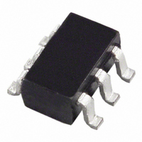
ADG602BRTZ-REEL7 Analog Devices Inc, ADG602BRTZ-REEL7 Datasheet - Page 6

ADG602BRTZ-REEL7
Manufacturer Part Number
ADG602BRTZ-REEL7
Description
IC,ANALOG SWITCH,SINGLE,SPST,CMOS,TSOP,6PIN,PLASTIC
Manufacturer
Analog Devices Inc
Type
Analog Switchr
Datasheet
1.ADG601BRMZ.pdf
(12 pages)
Specifications of ADG602BRTZ-REEL7
Package
6SOT-23
Maximum On Resistance
5@5V Ohm
Maximum High Level Output Current
100 mA
Maximum Turn-off Time
80@5V ns
Maximum Turn-on Time
220@5V ns
Switch Architecture
SPST
Power Supply Type
Single|Dual
Lead Free Status / RoHS Status
Lead free / RoHS Compliant
Available stocks
Company
Part Number
Manufacturer
Quantity
Price
Company:
Part Number:
ADG602BRTZ-REEL7
Manufacturer:
STM
Quantity:
4 995
ADG601/ADG602
PIN CONFIGURATIONS AND FUNCTION DESCRIPTIONS
Table 5. Pin Function Descriptions
6-Lead SOT-23
1
2
3
4
5
6
N/A
Table 6. Die Pad Coordinates
Die Pad No.
1
2
3
4
5
6
7
8
9
10
11
12
13
14
1
2
3
Measured from the center of the die.
Bond the D pads together to a single point to preserve the on resistance and current handling capability. The common point acts as the drain pin of the switch.
Bond the S pads together to a single point to preserve the on resistance and current handling capability. The common point acts as the source pin of the switch.
V
V
Figure 2. 6-Lead SOT-23 (RJ-6)
DD
SS
S
1
2
3
Pin No.
(Not to Scale)
ADG601/
ADG602
TOP VIEW
PIN 1
INDICATOR
8-Lead MSOP
4
8
5
7
1
6
2, 3
X (μm)
−265
−265
−265
−265
−265
−265
−265
−265
+265
+265
+265
+265
+265
+265
6
5
4
IN
D
GND
Coordinates
1
Die Pad
Mnemonic
V
S
V
GND
D
IN
NC
Y (μm)
+754
+525
+241
+141
−191
−409
−549
−787
−767
−429
−289
+189
+521
+661
DD
SS
Mnemonic
NC
D
D
D
NC
NC
NC
V
V
IN
GND
S
S
NC
DD
SS
Most Positive Power Supply Potential.
Source Terminal. Can be an input or output.
Most Negative Power Supply Potential.
Ground (0 V) Reference.
Drain Terminal. Can be an input or output.
Logic Control Input.
No Connect.
Description
V
NC
NC
DD
Figure 3. 8-Lead MSOP (RM-8)
D
Rev. C | Page 6 of 12
1
2
3
4
NC = NO CONNECT
(Not to Scale)
ADG601/
ADG602
TOP VIEW
PIN 1
INDICATOR
Description
No Connect.
Drain Terminal. Can be an input or output.
Drain Terminal. Can be an input or output.
Drain Terminal. Can be an input or output.
No Connect.
No Connect.
No Connect.
Most Positive Power Supply Potential.
Most Negative Power Supply Potential.
Logic Control Input.
Ground (0 V) Reference.
Source Terminal. Can be an input or output.
Source Terminal. Can be an input or output.
Source Terminal. Can be an input or output.
8
7
6
5
S
GND
IN
V
SS
Figure 4. Die (820 μm × 2255 μm)
1
2
3
4
5
6
7
8
(Not to Scale)
TOP VIEW
2
2
2
3
3
14
13
12
11
10
9


