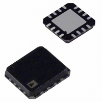
ADG633YCPZ Analog Devices Inc, ADG633YCPZ Datasheet - Page 5

ADG633YCPZ
Manufacturer Part Number
ADG633YCPZ
Description
2:1 MUX, +/-5V Supply Rate To +125? I.C.
Manufacturer
Analog Devices Inc
Datasheet
1.ADG633YRUZ.pdf
(16 pages)
Specifications of ADG633YCPZ
Function
Switch
Circuit
3 x SPDT
On-state Resistance
75 Ohm
Voltage Supply Source
Single, Dual Supply
Voltage - Supply, Single/dual (±)
2 V ~ 12 V, ±2 V ~ 6 V
Current - Supply
0.01µA
Operating Temperature
-40°C ~ 125°C
Mounting Type
Surface Mount
Package / Case
16-VQFN, CSP Exposed Pad
Lead Free Status / RoHS Status
Lead free / RoHS Compliant
Available stocks
Company
Part Number
Manufacturer
Quantity
Price
Part Number:
ADG633YCPZ-REEL7
Manufacturer:
ADI/亚德诺
Quantity:
20 000
V
Table 3.
Parameter
ANALOG SWITCH
LEAKAGE CURRENTS
DIGITAL INPUTS
DYNAMIC CHARACTERISTICS
POWER REQUIREMENTS
1
Guaranteed by design; not subject to production test.
DD
Analog Signal Range
On Resistance, R
On-Resistance Match
Source Off Leakage, I
Drain Off Leakage, I
Channel On Leakage, I
Input High Voltage, V
Input Low Voltage, V
Input Current, I
Digital Input Capacitance, C
t
t
t
Break-Before-Make Time Delay, t
Charge Injection
Off Isolation
Channel-to-Channel Crosstalk
−3 dB Bandwidth
C
C
C
I
DD
TRANSITION
ON
OFF
S(OFF)
D(OFF)
D(ON)
= 2.7 V to 3.6 V, V
Between Channels, ΔR
( EN )
( EN )
, C
S(ON)
INL
ON
or I
D(OFF)
INL
S(OFF)
INH
INH
D(ON)
SS
ON
= 0 V, GND = 0 V, T
, I
1
S(ON)
IN
BBM
+25°C
185
300
2
4.5
±0.005
±0.2
±0.005
±0.2
±0.005
±0.2
0.005
2
170
300
200
310
30
40
180
1
2
−90
−90
500
5
8
12
0.01
A
= −40°C to +125°C, unless otherwise noted.
B Version
−40°C to +85°C
350
6
370
380
55
Rev. A | Page 5 of 16
Y Version
−40°C to +125°C
0 to V
400
7
±5
±5
±5
2.0
0.5
±1
400
420
75
10
1
DD
Unit
V
Ω typ
Ω max
Ω typ
Ω max
nA typ
nA max
nA typ
nA max
nA typ
nA max
V min
V max
μA typ
μA max
pF typ
ns typ
ns max
ns typ
ns max
ns typ
ns max
ns typ
ns min
pC typ
pC max
dB typ
dB typ
MHz typ
pF typ
pF typ
pF typ
μA typ
μA max
Test Conditions/Comments
V
V
V
V
V
V
V
V
V
V
V
V
V
V
R
R
R
R
R
R
R
R
V
V
R
R
R
f = 1 MHz
f = 1 MHz
f = 1 MHz
V
Digital inputs = 0 V or 3.3 V
Digital inputs = 0 V or 3.3 V
L
L
L
DD
S
S
S
S
DD
S
S
S
S
S
S
IN
IN
L
L
L
L
L
L
S
S
L
L
DD
= 0 V to 2.7 V, I
= 0 V to 2.7 V, I
= 50 Ω, C
= +1.5 V, I
= +1.5 V, I
= 300 Ω, C
= 300 Ω, C
= 300 Ω, C
= 300 Ω, C
= 300 Ω, C
= 300 Ω, C
= 300 Ω, C
= 300 Ω, C
= 1.5 V, R
= 1.5 V, R
= 50 Ω, C
= 50 Ω, C
= 1 V/3 V, V
= 1 V/3 V, V
= 1 V/3 V, V
= 1 V/3 V, V
= V
= V
= V
= V
= 3.3 V
= 2.7 V, V
= 3.3 V
D
D
INL
INL
= 1 V or 3 V; see Figure 23
= 1 V or 3 V; see Figure 23
or V
or V
L
S
S
L
L
= 5 pF; see Figure 29
L
L
= 0 Ω, C
= 0 Ω, C
S
S
L
L
L
L
L
L
= 5 pF, f = 1 MHz; see Figure 28
= 5 pF, f = 1 MHz; see Figure 30
SS
INH
INH
= 35 pF, V
= 35 pF, V
= 0.1 mA
= 0.1 mA
D
D
D
D
= 35 pF, V
= 35 pF, V
= 35 pF, V
= 35 pF, V
= 35 pF, V
= 35 pF, V
= 0 V
= 3 V/1 V; see Figure 21
= 3 V/1 V; see Figure 21
= 3 V/1 V; see Figure 22
= 3 V/1 V; see Figure 22
S
S
= 0.1 mA; see Figure 20
= 0.1 mA; see Figure 20
L
L
= 1 nF; see Figure 27
= 1 nF; see Figure 27
S1
S1
S
S
S
S
S
S
= V
= V
= 1.5 V; see Figure 24
= 1.5 V; see Figure 24
= 1.5 V; see Figure 26
= 1.5 V; see Figure 26
= 1.5 V; see Figure 26
= 1.5 V; see Figure 26
S2
S2
= 1.5 V; see Figure 25
= 1.5 V; see Figure 25
ADG633


