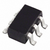
ADG701BRTZ-REEL7 Analog Devices Inc, ADG701BRTZ-REEL7 Datasheet

ADG701BRTZ-REEL7
Specifications of ADG701BRTZ-REEL7
Available stocks
Related parts for ADG701BRTZ-REEL7
ADG701BRTZ-REEL7 Summary of contents
Page 1
FEATURES 1 5.5 V single supply 2 Ω (typical) on resistance Low on resistance flatness –3 dB bandwidth > 200 MHz Rail-to-rail operation Fast switching times OFF Typical power consumption < ...
Page 2
ADG701/ADG702 TABLE OF CONTENTS Features .............................................................................................. 1 Applications....................................................................................... 1 Functional Block Diagram .............................................................. 1 General Description ......................................................................... 1 Product Highlights ........................................................................... 1 Revision History ............................................................................... 2 Specifications..................................................................................... 3 Absolute Maximum Ratings............................................................ 5 ESD Caution.................................................................................. 5 Pin Configurations and Function Descriptions ...
Page 3
SPECIFICATIONS ± 10%, GND = 0 V. Temperature range for B version is −40°C to +85°C, unless otherwise noted. DD Table 2. Parameter +25°C ANALOG SWITCH Analog Signal Range On Resistance ( ...
Page 4
ADG701/ADG702 ± 10%, GND = 0 V. Temperature range for B version is −40°C to +85°C, unless otherwise noted. DD Table 3. Parameter ANALOG SWITCH Analog Signal Range On Resistance ( Resistance Flatness ...
Page 5
ABSOLUTE MAXIMUM RATINGS T = +25°C, unless otherwise noted. A Table 4. Parameter V to GND DD 1 Analog and Digital Inputs Continuous Current Peak Current Operating Temperature Range Industrial (B Version) Storage Temperature ...
Page 6
ADG701/ADG702 PIN CONFIGURATIONS AND FUNCTION DESCRIPTIONS ADG701/ NC GND 2 7 ADG702 TOP VIEW (Not to Scale CONNECT Figure 2. 8-Lead MSOP Table 6. ...
Page 7
TYPICAL PERFORMANCE CHARACTERISTICS 3 2.7V DD 3.0 2 3.0V DD 2.0 1 5.0V DD 1.0 0 0.5 1.0 1.5 2.0 2.5 3 (DRAIN OR SOURCE VOLTAGE (V ...
Page 8
ADG701/ADG702 TERMINOLOGY Table 7. Term Description R Ohmic resistance between D and Flatness is defined as the difference between the maximum and minimum value of on resistance as measured over the FLAT(ON) specified analog signal range. I ...
Page 9
TEST CIRCUITS V1 Figure 11. On Resistance 0.1μ GND Figure ...
Page 10
ADG701/ADG702 APPLICATIONS INFORMATION The ADG701/ADG702 belong to the Analog Devices family of CMOS switches. This series of general-purpose switches has improved switching times, lower on resistance, higher bandwidth, low power consumption, and low leakage currents. ADG701/ADG702 SUPPLY VOLTAGES Functionality of ...
Page 11
OUTLINE DIMENSIONS INDICATOR 0.15 MAX 3.00 BSC 8 5 3.00 4.90 BSC BSC 1 4 PIN 1 0.65 BSC 1.10 MAX 0.15 0.00 8° 0.38 0.23 0° 0.22 0.08 COPLANARITY SEATING 0.10 PLANE COMPLIANT TO JEDEC STANDARDS MO-187-AA Figure 20. ...
Page 12
... ADG701BRMZ-REEL7 8-Lead Mini Small Outline Package [MSOP] 1 ADG701BRTZ-REEL 6-Lead Small Outline Transistor Package [SOT-23] 1 ADG701BRTZ-REEL7 6-Lead Small Outline Transistor Package [SOT-23] ADG702BRJ-500RL7 5-Lead Small Outline Transistor Package [SOT-23] ADG702BRJ-REEL 5-Lead Small Outline Transistor Package [SOT-23] ADG702BRJ-REEL7 5-Lead Small Outline Transistor Package [SOT-23] ...


