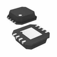
ADL5323ACPZ-R7 Analog Devices Inc, ADL5323ACPZ-R7 Datasheet

ADL5323ACPZ-R7
Specifications of ADL5323ACPZ-R7
Related parts for ADL5323ACPZ-R7
ADL5323ACPZ-R7 Summary of contents
Page 1
FEATURES Internally matched to 50 Ω input and output Internally biased Operating frequency: 1700 MHz to 2400 MHz Gain OIP3: 43 dBm P1 dB: 28 dBm Noise figure × LFCSP Power supply: ...
Page 2
ADL5323 TABLE OF CONTENTS Features .............................................................................................. 1 Applications....................................................................................... 1 Functional Block Diagram .............................................................. 1 General Description ......................................................................... 1 Revision History ............................................................................... 2 Specifications..................................................................................... 3 Absolute Maximum Ratings............................................................ 4 ESD Caution.................................................................................. 4 REVISION HISTORY 7/06—Revision 0: Initial Version Pin Configuration and ...
Page 3
SPECIFICATIONS 25° Table 1. Parameter Conditions FREQUENCY RANGE GAIN Frequency = 1960 MHz vs. Frequency 1930 MHz to 1990 MHz vs. Temperature −40°C to +85°C vs. Voltage 4. 5.25 V ...
Page 4
ADL5323 ABSOLUTE MAXIMUM RATINGS Table 2. Parameter Supply Voltage, VPOS Input Power (re: 50 Ω) Equivalent Voltage θ (Paddle Soldered) JC Maximum Junction Temperature Operating Temperature Range Storage Temperature Range Soldering Temperature ESD CAUTION ESD (electrostatic discharge) sensitive device. Electrostatic ...
Page 5
PIN CONFIGURATION AND FUNCTION DESCRIPTIONS Table 3. Pin Function Descriptions Pin No. Mnemonic Description VCC Positive 5 V Supply Voltage. Bypass these three pins with independent power supply decoupling networks (100 pF, 10 nF, and 10 μF). ...
Page 6
ADL5323 TYPICAL PERFORMANCE CHARACTERISTICS 23 TEMP = –40°C 22 TEMP = +25°C 21 TEMP = +85° 1700 1800 1900 2000 2100 FREQUENCY (MHz) Figure 4. Gain vs. Frequency ...
Page 7
OIP3 (dBm) Figure 10. Distribution of OIP3 at 1990 MHz –5 –10 –15 –20 S22 –25 S11 –30 –35 –40 1700 1800 1900 ...
Page 8
ADL5323 BASIC CONNECTIONS Figure 16 shows the basic connections for operating the ADL5323. Each of the three power supply lines should be decoupled with 10 μF, 10 nF, and 100 pF capacitors. Pin 3, Pin 6, Pin 7, and the ...
Page 9
EVALUATION BOARD Figure 18 shows the schematic of the ADL5323 evaluation board. The board is powered by a single supply in the 4. 5.25 V range. The power supply is decoupled on each of the three power supply ...
Page 10
... ADL5323 OUTLINE DIMENSIONS PIN 1 INDICATOR 0.90 MAX 0.85 NOM SEATING PLANE ORDERING GUIDE Model Temperature Range 1 ADL5323ACPZ-R7 −40°C to +85°C 1 ADL5323ACPZ-WP −40°C to +85°C ADL5323-EVAL Pb-free part. 3.00 0.60 MAX BSC SQ 8 2.75 TOP BSC SQ VIEW 0.50 BSC 5 0.70 MAX 12° ...
Page 11
NOTES Rev Page ADL5323 ...
Page 12
ADL5323 NOTES ©2006 Analog Devices, Inc. All rights reserved. Trademarks and registered trademarks are the property of their respective owners. D06058-0-7/06(0) Rev Page ...


