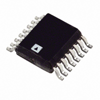
ADM2914-2ARQZ-RL7 Analog Devices Inc, ADM2914-2ARQZ-RL7 Datasheet - Page 5

ADM2914-2ARQZ-RL7
Manufacturer Part Number
ADM2914-2ARQZ-RL7
Description
Quad UV/OV Monitor
Manufacturer
Analog Devices Inc
Type
Multi-Voltage Supervisorr
Datasheet
1.EVAL-ADM2914EBZ.pdf
(16 pages)
Specifications of ADM2914-2ARQZ-RL7
Number Of Voltages Monitored
4
Output
Open Drain or Open Collector
Reset
Active Low
Reset Timeout
Adjustable/Selectable
Voltage - Threshold
Adjustable/Selectable
Operating Temperature
-40°C ~ 125°C
Mounting Type
Surface Mount
Package / Case
16-QSOP
Lead Free Status / RoHS Status
Lead free / RoHS Compliant
PIN CONFIGURATIONS AND FUNCTION DESCRIPTIONS
Table 4. Pin Function Descriptions
Pin No.
1
3
2
4
5
7
6
8
9
10
11
12
13
14
15
16
ADM2914-1
VH1
VH2
VL1
VL2
VH3
VH4
VL3
VL4
GND
REF
OV
UV
LATCH
SEL
TIMER
V
CC
Figure 2. ADM2914-1 Pin Configuration
VH1
VH2
VH3
VH4
VL1
VL2
VL3
VL4
Mnemonic
1
2
3
4
5
6
7
8
ADM2914-1
ADM2914-2
VH1
VH2
VL1
VL2
VH3
VH4
VL3
VL4
GND
REF
OV
UV
DIS
SEL
TIMER
V
(Not to Scale)
CC
TOP VIEW
16
15
14
13
12
11
10
9
Description
Voltage High Input 1 and Voltage High Input 2. If the voltage monitored by VH1 or VH2 drops
below 0.5 V, an undervoltage condition is detected. Connect to V
Voltage Low Input 1 and Voltage Low Input 2. If the voltage monitored by VL1 or VL2 rises above
0.5 V, an overvoltage condition is detected. Tie to GND when not in use.
Voltage High Input 3 and Voltage High Input 4. The polarity of these inputs is determined by the
state of the SEL pin (see Table 5). When the monitored input is configured as a positive voltage
and the voltage monitored by VH3 or VH4 drops below 0.5 V, an undervoltage condition is
detected. Conversely, when the input is configured as a negative voltage and the input drops
below 0.5 V, an overvoltage condition is detected. Connect to V
Voltage Low Input 3 and Voltage Low Input 4. The polarity of these inputs is determined by the
state of the SEL pin (see Table 5). When the monitored input is configured as a positive voltage
and the voltage monitored by VL3 or VL4 rises above 0.5 V, an overvoltage condition is detected.
Conversely, when the input is configured as a negative voltage and the input rises above 0.5 V, an
undervoltage condition is detected. Tie to GND when not in use.
Device Ground.
Buffered Reference Output. This pin is a 1 V reference that is used as an offset when monitoring
negative voltages. This pin can source or sink 1 mA, and drive loads up to 1 nF. Larger capacitive
loads may lead to instability. Leave unconnected when not in use.
Overvoltage Reset Output. OV is asserted low if a negative polarity input voltage drops below its
associated threshold or if a positive polarity input voltage exceeds its threshold. The ADM2914-1
allows OV to be latched low. The ADM2914-2 holds OV low for an adjustable timeout period
determined by the TIMER capacitor. This pin has a weak pull-up to VCC and can be pulled up to
16 V externally. Leave this pin unconnected when not in use.
Undervoltage Reset Output. UV is asserted low if a negative polarity input voltage exceeds its
associated threshold or if a positive polarity input voltage drops below its threshold. UV is held
low for an adjustable timeout period set by the external capacitor tied to the TIMER pin. The UV
pin has a weak pull-up to V
resistor. Leave this pin unconnected when not in use.
OV Latch Bypass Input/Clear Pin. When pulled high, the OV latch is cleared. When held high, the
OVoutput has the same delay and output characteristics as the UV output. When pulled low, the
OV output is latched when asserted. (Applies only to the ADM2914-1.)
OV and UV Disable Input. When pulled high, the OV and UV outputs are held high irrespective of
the state of the VHx and VLx input pins. However, if a UVLO condition occurs, the OV and UV
outputs are asserted. This pin has a weak internal pull-down (2 μA) to GND. Leave this pin
unconnected when not in use. (Applies only to the ADM2914-2.)
Input Polarity Select. This three-state input pin allows the polarity of VH3, VL3, VH4, and VL4 to be
configured. Connect to V
configurations (see Table 5).
Adjustable Reset Delay Timer. Connect an external capacitor to the TIMER pin to program the
reset timeout delay. Refer to Figure 15 in the Typical Performance Characteristics section.
Connect this pin to V
Supply Voltage. V
6 V, it operates as a shunt regulator. A dropper resistor must be used in this configuration to limit
the current to less than 10 mA. When used without the resistor, the voltage at this pin must not
exceed 6 V. A 0.1 μF bypass capacitor or greater should be used.
V
TIMER
SEL
LATCH
UV
OV
REF
GND
CC
CC
Rev. B | Page 5 of 16
operates as a direct supply for voltages up to 6 V. For voltages greater than
CC
to bypass the timer.
CC
CC
or GND, or leave open to select one of three possible input polarity
and can be pulled up to 16 V externally via an external pull-up
Figure 3. ADM2914-2 Pin Configuration
VH1
VH2
VH3
VH4
VL1
VL2
VL3
VL4
1
2
3
4
5
6
7
8
ADM2914-2
(Not to Scale)
TOP VIEW
CC
CC
when not in use.
when not in use.
16
15
14
13
12
11
10
9
V
TIMER
SEL
DIS
UV
OV
REF
GND
CC
ADM2914


