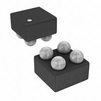
ADP150ACBZ-3.0-R7 Analog Devices Inc, ADP150ACBZ-3.0-R7 Datasheet - Page 12

ADP150ACBZ-3.0-R7
Manufacturer Part Number
ADP150ACBZ-3.0-R7
Description
150mA LDO 3.0Vout
Manufacturer
Analog Devices Inc
Datasheet
1.ADP150-BL1-EVZ.pdf
(20 pages)
Specifications of ADP150ACBZ-3.0-R7
Design Resources
Broadband Low EVM Direct Conversion Transmitter (CN0134) Broadband Low EVM Direct Conversion Transmitter Using LO Divide-by-2 Modulator (CN0144) Using low noise linear drop-out regulators to power wideband PLL & VCO IC's (CN0147)
Regulator Topology
Positive Fixed
Voltage - Output
3V
Voltage - Input
Up to 5.5V
Voltage - Dropout (typical)
0.105V @ 150mA
Number Of Regulators
1
Current - Output
150mA (Max)
Current - Limit (min)
190mA
Operating Temperature
-40°C ~ 125°C
Mounting Type
Surface Mount
Package / Case
4-WLCSP
Lead Free Status / RoHS Status
Lead free / RoHS Compliant
Other names
ADP150ACBZ-3.0-R7TR
ADP150
APPLICATIONS INFORMATION
CAPACITOR SELECTION
Output Capacitor
The ADP150 is designed for operation with small, space-saving
ceramic capacitors but functions with most commonly used
capacitors as long as care is taken with regard to the effective
series resistance (ESR) value. The ESR of the output capacitor
affects the stability of the LDO control loop. A minimum of 1 µF
capacitance with an ESR of 1 Ω or less is recommended to
ensure the stability of the ADP150. The transient response to
changes in load current is also affected by output capacitance.
Using a larger value of output capacitance improves the transient
response of the ADP150 to large changes in the load current.
Figure 27 and Figure 28 show the transient responses for output
capacitance values of 1 µF and 4.7 µF, respectively.
Input Bypass Capacitor
Connecting a 1 µF capacitor from VIN to GND reduces the
circuit sensitivity to the PCB layout, especially when long input
traces or high source impedance is encountered. If greater than
1 µF of output capacitance is required, increase the input capacitor
to match the output capacitor.
1
2
1
2
CH1 100mA CH2 50mV
CH1 100mA CH2 50mV
Figure 28. Output Transient Response, C
Figure 27. Output Transient Response, C
T
V
V
T
OUT
OUT
M1.0µs
M1.0µs
T
T
1mA TO 150mA LOAD STEP
1mA TO 150mA LOAD STEP
716.000µs
240.000ns
I
I
OUT
OUT
A CH1
A CH1
OUT
OUT
V
V
V
V
IN
OUT
IN
OUT
= 4.7 µF
= 1 µF
= 3.7V
= 3.7V
= 3.3V
= 3.3V
100mA
108mA
Rev. A | Page 12 of 20
Input and Output Capacitor Properties
Any good quality ceramic capacitors can be used with the ADP150,
as long as they meet the minimum capacitance and maximum
ESR requirements. Ceramic capacitors are manufactured with a
variety of dielectrics, each with different behavior over temperature
and applied voltage. Capacitors must have a dielectric adequate to
ensure the minimum capacitance over the necessary temperature
range and dc bias conditions. X5R or X7R dielectrics with a
voltage rating of 6.3 V or 10 V are recommended. Y5V and Z5U
dielectrics are not recommended, due to their poor temperature
and dc bias characteristics.
Figure 29 depicts the capacitance vs. the voltage bias characteristic
of a 0402, 1 µF, 10 V, X5R capacitor. The voltage stability of a
capacitor is strongly influenced by the capacitor size and voltage
rating. In general, a capacitor in a larger package or higher voltage
rating exhibits better stability. The temperature variation of the X5R
dielectric is about ±15% over the −40°C to +85°C temperature
range and is not a function of package or voltage rating.
Use Equation 1 to determine the worst-case capacitance,
accounting for capacitor variation over temperature, component
tolerance, and voltage.
where:
C
TEMPCO is the worst-case capacitor temperature coefficient.
TOL is the worst-case component tolerance.
In this example, the worst-case temperature coefficient (TEMPCO)
over −40°C to +85°C is assumed to be 15% for an X5R dielectric.
The tolerance of the capacitor (TOL) is assumed to be 10%, and
the C
Substituting these values in Equation 1 yields
Therefore, the capacitor chosen in this example meets the
minimum capacitance requirement of the LDO over temperature
and tolerance at the chosen output voltage.
BIAS
C
C
is the effective capacitance at the operating voltage.
BIAS
EFF
EFF
1.2
1.0
0.8
0.6
0.4
0.2
0
is 0.94 µF at 1.8 V, as shown in Figure 29.
= C
= 0.94 µF × (1 − 0.15) × (1 − 0.1) = 0.719 µF
Figure 29. Capacitance vs. Voltage Bias Characteristic
0
BIAS
× (1 − TEMPCO) × (1 − TOL)
2
BIAS VOLTAGE (V)
4
6
8
10
(1)


