ADP3605ARZ Analog Devices Inc, ADP3605ARZ Datasheet
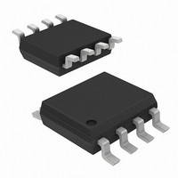
120mA Switched Capacitor Volt. Regulator

ADP3605ARZ

Manufacturer Part Number
ADP3605ARZ
Description
120mA Switched Capacitor Volt. Regulator
Manufacturer
Analog Devices Inc
Type
Switched Capacitor (Charge Pump), Invertingr
Datasheet

Specifications of ADP3605ARZ

Internal Switch(s)
Yes
Synchronous Rectifier
No
Number Of Outputs
1
Voltage - Output
-3 V ~ -6 V
Current - Output
120mA
Frequency - Switching
250kHz
Voltage - Input
3 V ~ 6 V
Operating Temperature
-40°C ~ 85°C
Mounting Type
Surface Mount
Package / Case
8-SOIC (0.154", 3.90mm Width)
Output Voltage
-3 to -6V
Output Current
120mA
Operating Supply Voltage (typ)
5V
Operating Supply Voltage (min)
3V
Operating Supply Voltage (max)
6V
Operating Temp Range
-40C to 85C
Operating Temperature Classification
Industrial
Package Type
SOIC N
Pin Count
8
Mounting
Surface Mount
Lead Free Status / RoHS Status
Lead free / RoHS Compliant
Lead Free Status / RoHS Status
Lead free / RoHS Compliant
Other names
Q4915857

Available stocks

Company
Part Number
Manufacturer
Quantity
Price
Part Number:
ADP3605ARZ
Manufacturer:
ADI/亚德诺
Quantity:
20 000
Part Number:
ADP3605ARZ-3
Manufacturer:
ADI
Quantity:
490
Part Number:
ADP3605ARZ-3
Manufacturer:
ADI/亚德诺
Quantity:
20 000
a
GENERAL DESCRIPTION
The ADP3605 is a 120 mA regulated output switched capacitor
voltage inverter. It provides a regulated output voltage with
minimum voltage loss and requires a minimum number of ex-
ternal components. In addition, the ADP3605 does not require
the use of an inductor.
Pin-for-pin and functionally compatible with the ADP3604, the
internal oscillator of the ADP3605 runs at 500 kHz nominal
frequency which produces an output switching frequency of
250 kHz. This allows for the use of smaller charge pump and
filter capacitors.
The ADP3605 provides an accuracy of 3% with a typical shut-
down current of 2 A. It can also operate from a single positive
input voltage as low as 3 V. The ADP3605 is offered with the
regulation fixed at –3 V or adjustable via external resistors over
a –3 V to –6 V range.
REV. A
Information furnished by Analog Devices is believed to be accurate and
reliable. However, no responsibility is assumed by Analog Devices for its
use, nor for any infringements of patents or other rights of third parties
which may result from its use. No license is granted by implication or
otherwise under any patent or patent rights of Analog Devices.
FEATURES
Fully Regulated Output Voltage (–3 V and Adjustable)
High Output Current: 120 mA
Output Accuracy:
250 kHz Switching Frequency
Low Shutdown Current: 2 A Typical
Input Voltage Range from 3 V to 6 V
SO-8 and RU-14 Packages
–40 C to +85 C Ambient Temperature Range
APPLICATIONS
Voltage Inverters
Voltage Regulators
Computer Peripherals and Add-On Cards
Portable Instruments
Battery Powered Devices
Pagers and Radio Control Receivers
Disk Drives
Mobile Phones
3%
Voltage Inverter with Regulated Output
One Technology Way, P.O. Box 9106, Norwood, MA 02062-9106, U.S.A.
Tel: 781/329-4700
Fax: 781/326-8703
V
SD
IN
V
120 mA Switched Capacitor
IN
ADP3605
CLOCK
4.7 F
Figure 1. Typical Application Circuit
OFF
*FOR BEST PERFORMANCE, 10 F IS RECOMMENDED
C
C
OSC
GEN
FUNCTIONAL BLOCK DIAGRAM
*C
P
IN
: SPRAGUE, 293D475X0010B2W
, C
IN
+
O
: TOKIN, 1E475ZY5UC205F
S D
ON
0
P
4.7 F
World Wide Web Site: http://www.analog.com
S1
*C
SD
P
C
S
+
P
+
N
D
S2
ADP3605-3
V
C
C
IN
P
P
+
C
GND
P
V
OUT
S4
© Analog Devices, Inc., 1999
D
FEEDBACK
CONTROL
N
ADP3605
LOOP
S
D
GND
N
V
B
SENSE
S
S3
+
*C
4.7 F
O
–3.0V
V
V
OUT
SENSE

Related parts for ADP3605ARZ

ADP3605ARZ Summary of contents

Page 1

FEATURES Fully Regulated Output Voltage (–3 V and Adjustable) High Output Current: 120 mA Output Accuracy: 3% 250 kHz Switching Frequency Low Shutdown Current Typical Input Voltage Range from SO-8 and RU-14 ...

Page 2

ADP3605–SPECIFICATIONS Parameter OPERATING SUPPLY RANGE SUPPLY CURRENT Shutdown Mode 4 OUTPUT VOLTAGE LOAD REGULATION OUTPUT RESISTANCE Open Loop OUTPUT RIPPLE VOLTAGE SWITCHING FREQUENCY SHUTDOWN Logic Input High Input Current Logic Input Low Input Current NOTES 1 Capacitors C C and ...

Page 3

Table I. Other Members of ADP36xx Family Output Package 2 Model Current Option ADP3603AR 50 mA SO-8 ADP3604AR 120 mA SO-8 ADP3610ARU 320 mA TSSOP-16 Nom. 3.3 V NOTES 1 See individual data sheets for detailed ordering information ...

Page 4

ADP3605 –Typical Performance Characteristics 270 260 250 3 3.5 4 4.5 5 5.5 SUPPLY VOLTAGE – Volts Figure 2. Oscillator Frequency vs. Supply Voltage 300 280 260 240 220 200 –40 – TEMPERATURE – C Figure 5. ...

Page 5

THEORY OF OPERATION The ADP3605 uses a switched capacitor principle to generate a negative voltage from a positive input voltage. An onboard oscillator generates a two phase clock to control a switching network that transfers charge between the storage capacitors. ...

Page 6

ADP3605 Pump Capacitor The ADP3605 alternately charges C to the input voltage when switched in parallel with the input supply, and then trans- P fers charge to C when C is switched in parallel with C O ...

Page 7

Maximum Output Voltage Maximum unregulated output voltage can be obtained on the ADP3605-3 by connecting the V SENSE to the V pin. Under this condition, the magnitude of the OUT unregulated output voltage depends on the load current ...

Page 8

ADP3605 8-Lead Small Outline IC (SO-8) 0.1968 (5.00) 0.1890 (4.80 0.1574 (4.00) 0.2440 (6.20 0.1497 (3.80) 0.2284 (5.80) PIN 1 0.0688 (1.75) 0.0098 (0.25) 0.0532 (1.35) 0.0040 (0.10) 0.0500 0.0192 (0.49) SEATING 0.0098 (0.25) (1.27) 0.0138 ...

Related keywords