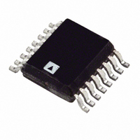
ADT7516ARQZ-REEL7 Analog Devices Inc, ADT7516ARQZ-REEL7 Datasheet - Page 5

ADT7516ARQZ-REEL7
Manufacturer Part Number
ADT7516ARQZ-REEL7
Description
IC,TEMPERATURE SENSOR,CMOS,SSOP,16PIN,PLASTIC
Manufacturer
Analog Devices Inc
Datasheet
1.ADT7517ARQZ.pdf
(44 pages)
Specifications of ADT7516ARQZ-REEL7
Function
Temp Monitoring System (Sensor)
Topology
ADC, Comparator, Multiplexer, Register Bank
Sensor Type
External & Internal
Sensing Temperature
-40°C ~ 120°C, External Sensor
Output Type
I²C™, MICROWIRE™, QSPI™, SPI™
Output Alarm
No
Output Fan
No
Voltage - Supply
2.7 V ~ 5.5 V
Operating Temperature
-40°C ~ 120°C
Mounting Type
Surface Mount
Package / Case
16-QSOP
Lead Free Status / RoHS Status
Lead free / RoHS Compliant
For Use With
EVAL-ADT7516EBZ - BOARD EVALUATION FOR ADT7516
Lead Free Status / RoHS Status
Lead free / RoHS Compliant
Parameter
ON-CHIP REFERENCE
OUTPUT CHARACTERISTICS
DIGITAL INPUTS
DIGITAL OUTPUT
I
SPI TIMING CHARACTERISTICS
POWER REQUIREMENTS
2
C TIMING CHARACTERISTICS
Reference Voltage
Temperature Coefficient
Output Voltage
DC Output Impedance
Short Circuit Current
Power-Up Time
Input Current
V
V
Pin Capacitance
SCL, SDA Glitch Rejection
LDAC Pulse Width
Digital High Voltage, V
Output Low Voltage, V
Output High Current, I
Output Capacitance, C
INT/INT Output Saturation Voltage
Serial Clock Period, t
Data In Setup Time to SCL High, t
Data Out Stable after SCL Low, t
SDA Low Setup Time to SCL
SDA High Hold Time after SCL
SDA and SCL Fall Time, t
SDA and SCL Rise Time, t
CS to SCLK Setup Time, t
SCLK High Pulse Width, t
SCLK Low Pulse Width, t
Data Access Time after SCLK
Data Setup Time Prior to SCLK
Data Hold Time after SCLK
CS to SCLK Hold Time, t
CS to DOUT High Impedance, t
V
V
I
DD
IL
IH
DD
DD
, Input Low Voltage
Low (Start Condition), t
High (Stop Condition), t
Falling Edge, t
Rising Edge, t
Rising Edge, t
, Input High Voltage
(Normal Mode)
Settling Time
1
4
6
5
6
4
11
4
12
1
OH
OL
OH
OUT
7
6
3
4
1
7
2
4
4
5
7, 8
4, 10
8
3
2
Min
2.2662
0.001
1.89
20
2.4
2.5
50
0
50
50
0
50
50
20
0
0
2.7
Typ
2.28
80
0.5
25
16
5
3
2.2
2.5
Max
2.2938
V
±1
0.8
10
50
0.4
1
50
0.8
300
300
35
40
5.5
50
3
3
DD
Rev. B | Page 5 of 44
− 0.1
9
Unit
V
ppm/°C
V
Ω
mA
mA
μs
μs
μA
V
V
pF
ns
ns
V
V
mA
pF
V
μs
ns
ns
ns
ns
ns
ns
ns
ns
ns
ns
ns
ns
μs
ns
V
ms
mA
mA
Conditions/Comments
This is a measure of the minimum and maximum
drive capability of the output amplifier
V
V
Coming out of power-down mode, V
Coming out of power-down mode, V
V
All digital inputs
Input filtering suppresses noise spikes of less
than 50 ns
Edge triggered input
I
I
V
I
Fast mode I
See Figure 2
See Figure 2
See Figure 2
See Figure 2
See Figure 2
See Figure 3
See Figure 3
See Figure 3
See Figure 3
See Figure 3
See Figure 3
See Figure 3
V
V
V
SOURCE
OL
OUT
DD
DD
IN
OH
DD
DD
DD
= 3 mA
= 0 V to V
= 5 V
= 3 V
= 5 V
= 4 mA
settles to within 10% of its final voltage level
= 3.3 V, V
= 5 V, V
ADT7516/ADT7517/ADT7519
= I
SINK
IH
2
= 200 μA
C, see Figure 2
DD
IH
= V
= V
DD
DD
, and V
, and V
IL
= GND
IL
= GND
DD
DD
= 5 V
= 3.3 V


