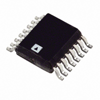
ADT7519ARQZ-REEL Analog Devices Inc, ADT7519ARQZ-REEL Datasheet - Page 20

ADT7519ARQZ-REEL
Manufacturer Part Number
ADT7519ARQZ-REEL
Description
IC,TEMPERATURE SENSOR,CMOS,SSOP,16PIN,PLASTIC
Manufacturer
Analog Devices Inc
Datasheet
1.ADT7517ARQZ.pdf
(44 pages)
Specifications of ADT7519ARQZ-REEL
Function
Temp Monitoring System (Sensor)
Topology
ADC, Comparator, Multiplexer, Register Bank
Sensor Type
External & Internal
Sensing Temperature
-40°C ~ 120°C, External Sensor
Output Type
I²C™, MICROWIRE™, QSPI™, SPI™
Output Alarm
No
Output Fan
No
Voltage - Supply
2.7 V ~ 5.5 V
Operating Temperature
-40°C ~ 120°C
Mounting Type
Surface Mount
Package / Case
16-QSOP
Lead Free Status / RoHS Status
Lead free / RoHS Compliant
ADT7516/ADT7517/ADT7519
The ADT7516/ADT7517/ADT7519 power up with averaging
on. This means every channel is measured 16 times and inter-
nally averaged to reduce noise. The conversion time can also be
sped up by turning off the averaging. This is done by setting
Bit C5 of the Control Configuration 2 register (Address 0x19) to 1.
FUNCTION DESCRIPTION—VOLTAGE OUTPUT
Digital-to-Analog Converters
The ADT7516/ADT7517/ADT7519 have four resistor string
DACs fabricated on a CMOS process with resolutions of 12, 10,
and 8 bits, respectively. They contain four output buffer amplifiers
and are written to via I
See the Serial Interface section for more information.
The ADT7516/ADT7517/ADT7519 operate from a single
supply of 2.7 V to 5.5 V, and the output buffer amplifiers
provide rail-to-rail output swing with a slew rate of 0.7 V/μs. All
four DACs share a common reference input, V
reference input is buffered to draw virtually no current from the
reference source because it offers the source a high impedance
input. The devices have a power-down mode to completely turn
off all DACs with a high impedance output.
Each DAC output is not updated until it receives the LDAC
command. Therefore, though the DAC registers would have
been written to with a new value, this value is not represented
by a voltage output until the DACs receive the LDAC command.
Reading back from any DAC register prior to issuing an LDAC
command results in the digital value that corresponds to the
DAC output voltage. Thus, the digital value written to the DAC
register cannot be read back until after the LDAC command has
been initiated. This LDAC command can be given by either
pulling the LDAC pin low (falling edge loads DACs), setting up
Bit D4 and Bit D5 of the DAC configuration register
(Address 0x1B), or using the LDAC register (Address 0x1C).
When using the LDAC pin to control the DAC register loading,
the low going pulse width should be 20 ns minimum. The
LDAC pin has to go high and low again before the DAC
registers can be reloaded.
Digital-to-Analog Section
The architecture of one DAC channel consists of a resistor string
DAC followed by an output buffer amplifier. The voltage at the
V
reference voltage for the corresponding DAC. Figure 42 shows a
block diagram of the DAC architecture. Because the input
coding to the DAC is straight binary, the ideal output voltage is
given by
where:
D = decimal equivalent of the binary code that is loaded to the
DAC register
REF
-IN pin or the on-chip reference of 2.28 V provides the
V
OUT
=
V
REF
2
N
×
D
2
C serial interface or SPI serial interface.
REF
-IN. The
Rev. B | Page 20 of 44
N = DAC resolution.
Resistor String
The resistor string section is shown in Figure 43. It is simply a
string of resistors, each of approximately 603 Ω. The digital
code loaded to the DAC register determines at which node on
the string the voltage is tapped off to be fed into the output
amplifier. The voltage is tapped off by closing one of the
switches connecting the string to the amplifier. Because it is a
string of resistors, it is guaranteed monotonic.
0 to 255 for ADT7519 (8 bits)
0 to 1023 for ADT7517 (10 bits)
0 to 4095 for ADT7516 (12 bits)
REGISTER
INPUT
Figure 42. Single DAC Channel Architecture
INTERNAL V
Figure 44. DAC Reference Buffer Circuit
REGISTER
R
R
R
R
R
INT V
DAC
2.28V
Figure 43. Resistor String
REF
REF
RESISTOR
V
STRING
REF
TO OUTPUT
AMPLIFIER
-IN
STRING
STRING
STRING
STRING
DAC A
DAC B
DAC C
DAC D
REFERENCE
BUFFER
V
OUTPUT BUFFER
REF
(GAIN = 1 OR 2)
GAIN MODE
AMPLIFIER
-IN
V
OUT
-A


