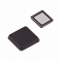
ADUC7020BCPZ62I-RL Analog Devices Inc, ADUC7020BCPZ62I-RL Datasheet - Page 89

ADUC7020BCPZ62I-RL
Manufacturer Part Number
ADUC7020BCPZ62I-RL
Description
IC,MICROCONTROLLER,16-BIT,ARM7 CPU,CMOS,LLCC,40PIN,PLASTIC
Manufacturer
Analog Devices Inc
Series
MicroConverter® ADuC7xxxr
Datasheet
1.USB-I2CLIN-CONV-Z.pdf
(96 pages)
Specifications of ADUC7020BCPZ62I-RL
Core Processor
ARM7
Core Size
16/32-Bit
Speed
44MHz
Connectivity
EBI/EMI, I²C, SPI, UART/USART
Peripherals
PLA, PWM, PSM, Temp Sensor, WDT
Number Of I /o
14
Program Memory Size
62KB (62K x 8)
Program Memory Type
FLASH
Ram Size
8K x 8
Voltage - Supply (vcc/vdd)
2.7 V ~ 3.6 V
Data Converters
A/D 5x12b; D/A 4x12b
Oscillator Type
Internal
Operating Temperature
-40°C ~ 125°C
Package / Case
40-LFCSP
Lead Free Status / RoHS Status
Lead free / RoHS Compliant
For Use With
EVAL-ADUC7020QSZ - KIT DEV ADUC7020 QUICK STARTEVAL-ADUC7020MKZ - KIT MINI DEV FOR ADUC7026/7027
Eeprom Size
-
Lead Free Status / RoHS Status
Lead free / RoHS Compliant
Available stocks
Company
Part Number
Manufacturer
Quantity
Price
Part Number:
ADUC7020BCPZ62I-RL
Manufacturer:
ADI/亚德诺
Quantity:
20 000
POWER-ON RESET OPERATION
An internal power-on reset (POR) is implemented on the
ADuC7019/20/21/22/24/25/26/27/28/29. For LV
typical, the internal POR holds the part in reset. As LV
above 2.35 V, an internal timer times out for, typically, 128 ms
before the part is released from reset. The user must ensure that
the power supply IOV
by this time. Likewise, on power-down, the internal POR holds
the part in reset until LV
Figure 82 illustrates the operation of the internal POR in detail.
TYPICAL SYSTEM CONFIGURATION
A typical ADuC7020 configuration is shown in Figure 83. It summarizes some of the hardware considerations discussed in the previous
sections. The bottom of the CSP package has an exposed pad that must be soldered to a metal plate on the board for mechanical reasons.
The metal plate of the board can be connected to ground.
1kΩ
1
2
3
4
5
6
7
8
9
10
11
12
13
14
15
16
17
18
19
20
DV
DD
+
–
TRST
TDI
TMS
TCK
TDO
DD
DD
reaches a stable 2.7 V minimum level
DV
DD
drops below 2.35 V.
DV
10Ω
DD
0.01µF
10
1
2
3
4
5
6
7
8
9
GND
DAC0
TMS
TDI
P0.0
40
11
39
12
REF
38
13
ADuC7020
AV
37
14
DD
36
15
DD
0.47µF
DV
0.47µF
35
16
below 2.35 V
DD
34
17
Figure 83. Typical System Configuration
33
18
DD
XCLKO
XCLKI
32
19
rises
31
20
Rev. C | Page 89 of 96
30
29
28
27
26
25
24
23
22
21
DV
DD
1kΩ
32.768kHz
ADuC7019/20/21/22/24/25/26/27/28/29
RS232 INTERFACE*
* EXTERNAL UART TRANSCEIVER INTEGRATED IN SYSTEM OR AS
PART OF AN EXTERNAL DONGLE AS DESCRIBED IN uC006.
AV
DD
10µF
1.5Ω
IOV
LV
POR
RST
DD
DD
1
2
3
4
5
6
7
8
270Ω
C1+
V+
C1–
C2+
C2–
V–
T2
R2
2.35V TYP
Figure 82. Internal Power-On Reset Operation
ADM3202
OUT
IN
DV
DD
10µF
R1
R2
T1
GND
R1
T1
T2
V
OUT
OUT
OUT
CC
NOT CONNECTED IN THIS EXAMPLE
IN
IN
IN
ADP3333-3.3
16
15
14
13
12
11
10
9
OUT
GND
SD
IN
128ms TYP
0.12ms TYP
0.1µF
STANDARD D-TYPE
3.3V
2.6V
CONNECTOR TO
SERIAL COMMS
PC HOST
1
2
3
4
5
6
7
8
9
2.35V TYP


