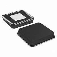
ADUC7061BCPZ32 Analog Devices Inc, ADUC7061BCPZ32 Datasheet - Page 18

ADUC7061BCPZ32
Manufacturer Part Number
ADUC7061BCPZ32
Description
DUAL 24-BIT AFE AND ARM 7 I.C
Manufacturer
Analog Devices Inc
Series
MicroConverter® ADuC7xxxr
Datasheet
1.EVAL-ADUC7061MKZ.pdf
(108 pages)
Specifications of ADUC7061BCPZ32
Design Resources
USB Based Temperature Monitor Using ADuC7061 and an External RTD (CN0075) 4 mA-to-20 mA Loop-Powered Temperature Monitor Using ADuC7060/1 (CN0145)
Core Processor
ARM7
Core Size
16/32-Bit
Speed
10MHz
Connectivity
I²C, SPI, UART/USART
Peripherals
POR, PWM, Temp Sensor, WDT
Number Of I /o
8
Program Memory Size
32KB (32K x 8)
Program Memory Type
FLASH
Ram Size
4K x 8
Voltage - Supply (vcc/vdd)
2.375 V ~ 2.625 V
Data Converters
A/D 5x24b, 8x24b, D/A 1x14b
Oscillator Type
Internal
Operating Temperature
-40°C ~ 125°C
Package / Case
32-LFCSP
Package
32LFCSP EP
Device Core
ARM7TDMI
Family Name
ADuC7xxx
Maximum Speed
10.24 MHz
Operating Supply Voltage
2.5 V
Data Bus Width
16|32 Bit
Number Of Programmable I/os
14
Interface Type
I2C/SPI/UART
On-chip Adc
2(4-chx24-bit)
Number Of Timers
4
Lead Free Status / RoHS Status
Lead free / RoHS Compliant
Eeprom Size
-
Lead Free Status / RoHS Status
Lead free / RoHS Compliant
Available stocks
Company
Part Number
Manufacturer
Quantity
Price
Company:
Part Number:
ADUC7061BCPZ32
Manufacturer:
AD
Quantity:
3 100
Company:
Part Number:
ADUC7061BCPZ32
Manufacturer:
ADI
Quantity:
538
Part Number:
ADUC7061BCPZ32
Manufacturer:
ADI/亚德诺
Quantity:
20 000
ADuC7060/ADuC7061
Table 9. ADuC7061 Pin Function Descriptions
Pin No.
1
2
3
4
5
6
7
8
9
10
11
12
13
14
15
16
17
18
19
20
0
Mnemonic
RESET
TMS
P1.0/IRQ1/SIN/T0
P1.1/SOUT
DAC0
ADC5/EXT_REF2IN−
ADC4/EXT_REF2IN+
ADC3
ADC2
IEXC1
IEXC0
GND_SW
ADC1
ADC0
AGND
AVDD
VREF+
VREF−
P0.0/SS/ADC6
P0.1/SCLK/SCL/ADC7
EP
Type
I
I
I/O
I/O
O
I
I
I
I
O
O
I
I
I
S
S
I
I
I/O
I/O
ADC5/EXT_REF2IN−
ADC4/EXT_REF2IN+
NOTES
1. THE 32-LEAD LFCSP_VQ HAS AN EXPOSED PADDLE. THIS EXPOSED
1
PADDLE MUST BE LEFT UNCONNECTED.
P1.0/IRQ1/SIN/T0
Description
Reset Pin. Input pin, active low. An external 1 kΩ pull-up resistor is recommended with this pin.
JTAG Test Mode Select. Input pin used for debug and download. An external pull-up resistor
(~100 kΩ) should be added to this pin.
General-Purpose Input and General-Purpose Output P1.0/External Interrupt Request 1/Serial
Input/Timer0 Input. This is a multifunction input/output pin offering four functions.
General-Purpose Input and General-Purpose Output P1.1/Serial Output. This is a dual function
input/output pin.
DAC Output. Analog output pin.
Single-Ended or Differential Analog Input 5/External Reference Negative Input. This is a dual
function analog input pin. The ADC5 serves as the analog input for the auxiliary ADC. The
EXT_REF2IN− serves as the external reference negative input by ADC for the auxiliary channel.
Multifunction Analog Input Pin. This pin can be used for the single-ended or differential Analog
Input 4, which is the analog input for the auxiliary ADC, or it can be used for the external
reference positive input for the auxiliary channel.
Single-Ended or Differential Analog Input 3. Analog input for primary and auxiliary ADCs.
Single-Ended or Differential Analog Input 2. Analog input for primary and auxiliary ADCs.
Programmable Current Source. Analog output pin.
Programmable Current Source. Analog output pin.
Switch to Internal Analog Ground Reference. When this input pin is not used, connect it directly
to the AGND system ground.
Single-Ended or Differential Analog Input 1. Analog input for the primary ADC. Negative differential
input for primary ADC.
Single-Ended or Differential Analog Input 0. Analog input for the primary ADC. Positive differential
input for primary ADC.
Analog Ground.
Analog Supply Pin.
External Reference Positive Input for the Primary Channel. Analog input pin.
External Reference Negative Input for the Primary Channel. Analog input pin.
General-Purpose Input and General-Purpose Output P0.0/SPI Slave Select (Active Low)/Input to
Auxiliary ADC6. This is a multifunction input/output pin. Single-ended or differential Analog
Input 6. Analog input for the auxiliary ADC.
General-Purpose Input and General-Purpose Output P0.1/SPI Clock/I
ADC7. This is a multifunction input/output pin. Single-ended or differential Analog Input 7.
Analog input for the auxiliary ADC.
Exposed Paddle. The 32-lead LFCSP_VQ has an exposed paddle that must be left unconnected.
P1.1/SOUT
RESET
DAC0
ADC3
TMS
Figure 8. 32-Lead LFCSP Pin Configuration
1
2
3
4
5
6
7
8
Rev. B | Page 18 of 108
ADuC7061
(Not to Scale)
PIN 1
INDICATOR
TOP VIEW
24 XTALI
23 XTALO
22 P0.3/MOSI/SDA/ADC9
21 P0.2/MISO/ADC8
20 P0.1/SCLK/SCL/ADC7
19 P0.0/SS/ADC6
18 VREF–
17 VREF+
2
C Clock/Input to Auxiliary


