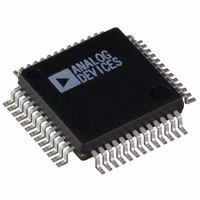
ADUC824BSZ Analog Devices Inc, ADUC824BSZ Datasheet - Page 28

ADUC824BSZ
Manufacturer Part Number
ADUC824BSZ
Description
IC,Data Acquisition CODEC,2-CHANNEL,QFP,52PIN,PLASTIC
Manufacturer
Analog Devices Inc
Series
MicroConverter® ADuC8xxr
Specifications of ADUC824BSZ
Core Processor
8052
Core Size
8-Bit
Speed
12.58MHz
Connectivity
EBI/EMI, I²C, SPI, UART/USART
Peripherals
POR, PSM, Temp Sensor, WDT
Number Of I /o
34
Program Memory Size
8KB (8K x 8)
Program Memory Type
FLASH
Eeprom Size
640 x 8
Ram Size
256 x 8
Voltage - Supply (vcc/vdd)
2.7 V ~ 5.25 V
Data Converters
A/D 3x16b, 4x24b; D/A 1x12b
Oscillator Type
Internal
Operating Temperature
-40°C ~ 85°C
Package / Case
52-MQFP, 52-PQFP
Cpu Family
ADuC8xx
Device Core
8052
Device Core Size
8b
Frequency (max)
12.58MHz
Interface Type
I2C/SPI/UART
Total Internal Ram Size
256Byte
# I/os (max)
26
Number Of Timers - General Purpose
3
Operating Supply Voltage (typ)
3.3/5V
Operating Supply Voltage (max)
5.25V
Operating Supply Voltage (min)
2.7V
On-chip Adc
2(2-chx24-bit)
On-chip Dac
1-chx12-bit
Instruction Set Architecture
CISC
Operating Temp Range
-40C to 85C
Operating Temperature Classification
Industrial
Mounting
Surface Mount
Pin Count
52
Package Type
MQFP
Lead Free Status / RoHS Status
Lead free / RoHS Compliant
Lead Free Status / RoHS Status
Lead free / RoHS Compliant, Lead free / RoHS Compliant
Available stocks
Company
Part Number
Manufacturer
Quantity
Price
Company:
Part Number:
ADUC824BSZ
Manufacturer:
INTEL
Quantity:
19
Company:
Part Number:
ADUC824BSZ
Manufacturer:
ADI
Quantity:
329
Company:
Part Number:
ADUC824BSZ
Manufacturer:
Analog Devices Inc
Quantity:
10 000
Part Number:
ADUC824BSZ
Manufacturer:
ADI/亚德诺
Quantity:
20 000
Company:
Part Number:
ADUC824BSZ-REEL
Manufacturer:
Analog Devices Inc
Quantity:
10 000
ADuC824
ADC1CON (Auxiliary ADC Control Register)
Used to configure the Auxiliary ADC for channel selection, external Ref enable and unipolar or bipolar coding. It should be noted that the
Auxiliary ADC only operates on a fixed input range of ± V
SFR Address
Power-On Default Value
Bit Addressable
Bit
7
6
5
4
3
2
1
0
*NOTES
1. When the temperature sensor is selected, user code must select internal reference via XREF1 bit above and clear the UNI1 bit (ADC1CON.3) to select bipolar coding.
2. The temperature sensor is factory calibrated to yield conversion results 8000H at 0 °C.
3. A +1°C change in temperature will result in a +1 LSB change in the ADC1H register ADC conversion result.
SF (Sinc Filter Register)
The number in this register sets the decimation factor and thus
the output update rate for the Primary and Auxiliary ADCs.
This SFR cannot be written by user software while either ADC is
active. The update rate applies to both Primary and Auxiliary
ADCs and is calculated as follows:
Where:
The allowable range for SF is 0Dhex to FFhex. Examples of SF
values and corresponding conversion update rate (f
—
f
f
SF =
ADC
MOD
Name
—
XREF1
ACH1
ACH0
UNI1
—
—
—
=
= Modulator Clock Frequency = 32.768 kHz
f
X
ADC
ADC Output Update Rate
Decimal Value of SF Register
R
E
=
F
1
3
1
×
8
.
SF
1
Auxiliary ADC External Reference Bit
Auxiliary ADC Channel Selection Bits
D3H
00H
No
Description
Reserved for Future Use
Set by user to enable the Auxiliary ADC to use the external reference via REFIN(+)/REFIN(–).
Cleared by user to enable the Auxiliary ADC to use the internal bandgap reference.
Written by the user to select the single-ended input pins used to drive the Auxiliary ADC as follows:
ACH1
0
0
1
1
Auxiliary ADC Unipolar Bit
Set by user to enable unipolar coding, i.e., zero input will result in 0000 hex output.
Cleared by user to enable bipolar coding, zero input will result in 8000 hex output.
Reserved for Future Use
Reserved for Future Use
Reserved for Future Use
×
A
f
C
MOD
H
1
Table VI. ADC1CON SFR Bit Designations
ACH0
0
1
0
1
ADC
) and con-
A
C
REF
H
0
.
Positive Input
AIN3
AIN4
Temp Sensor*
AIN5
–28–
version time (t
value for the SF register is 45hex, resulting in a default ADC
update rate of just under 20 Hz. Both ADC inputs are chopped
to minimize offset errors, which means that the settling time for
a single conversion or the time to a first conversion result in
continuous conversion mode is 2 × t
all calibration cycles will be carried out automatically with a
maximum, i.e., FFhex, SF value to ensure optimum calibra-
tion performance. Once a calibration cycle has completed, the
value in the SF register will be that programmed by user software.
SF(dec)
13
69
255
U
N
1 I
Negative Input
AGND
AGND
AGND (Temp. Sensor routed to the ADC input)
AGND
Table VII. SF SFR Bit Designations
ADC
) are shown in Table VII, the power-on default
SF(hex)
FF
0D
45
—
f
105.3
19.79
5.35
ADC
ADC
—
. As mentioned earlier,
(Hz)
t
9.52
50.34
186.77
ADC
—
REV. B
(ms)


