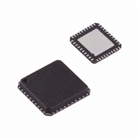
ADV3003ACPZ Analog Devices Inc, ADV3003ACPZ Datasheet - Page 3

ADV3003ACPZ
Manufacturer Part Number
ADV3003ACPZ
Description
IC,Cable Equalizer,LLCC,40PIN,PLASTIC
Manufacturer
Analog Devices Inc
Datasheet
1.ADV3003ACPZ-R7.pdf
(16 pages)
Specifications of ADV3003ACPZ
Applications
DVI, HDMI Equalizer/Driver
Interface
TMDS
Voltage - Supply
3 V ~ 3.6 V
Package / Case
40-LFCSP
Mounting Type
Surface Mount
Lead Free Status / RoHS Status
Lead free / RoHS Compliant
Lead Free Status / RoHS Status
Lead free / RoHS Compliant
Available stocks
Company
Part Number
Manufacturer
Quantity
Price
Company:
Part Number:
ADV3003ACPZ
Manufacturer:
Analog Devices Inc
Quantity:
135
Company:
Part Number:
ADV3003ACPZ
Manufacturer:
TI
Quantity:
30
Part Number:
ADV3003ACPZ
Manufacturer:
ADI/亚德诺
Quantity:
20 000
SPECIFICATIONS
T
data rate = 2.25 Gbps, TMDS outputs terminated with external 50 Ω resistors to 3.3 V, unless otherwise noted.
Table 1.
Parameter
DYNAMIC PERFORMANCE
EQUALIZATION PERFORMANCE
INPUT CHARACTERISTICS
OUTPUT CHARACTERISTICS
TERMINATION
POWER SUPPLY
QUIESCENT CURRENT
POWER DISSIPATION
PARALLEL CONTROL INTERFACE
1
2
3
4
5
6
Differential interpair skew is measured between the TMDS pairs of the HDMI/DVI link.
ADV3003 output meets the transmitter eye diagram mask as defined in the HDMI Standard Version 1.3a and the DVI Standard Version 1.0.
Cable output meets the receiver eye diagram mask as defined in the HDMI Standard Version 1.3a and the DVI Standard Version 1.0.
PE = 0 dB.
Typical value assumes the HDMI/DVI link is active with nominal signal swings. Minimum and maximum limits are measured at the extremes of input termination
resistance and input voltage swing, respectively .
The total power dissipation excludes power dissipated in the 50 Ω off-chip loads.
A
Maximum Data Rate (DR) per Channel
Bit Error Rate (BER)
Added Deterministic Jitter
Added Random Jitter
Differential Intrapair Skew
Differential Interpair Skew
Receiver (Fixed Setting)
Transmitter (Pre-Emphasis On)
Input Voltage Swing
Input Common-Mode Voltage (V
High Voltage Level
Low Voltage Level
Rise/Fall Time (20% to 80%)
Input Termination Resistance
Output Termination Resistance
AVCC
AVCC
VTTI
VTTO
Input High Voltage, V
Input Low Voltage, V
= 27°C, AVCC = 3.3 V, VTTI = 3.3 V, VTTO = 3.3 V, AVEE = 0 V, differential input swing = 1000 mV, pattern = PRBS 2
6
IL
IH
2
4
1
3
ICM
)
DR ≤ 2.25 Gbps, PRBS 2
Conditions/Comments
NRZ
PRBS 2
At output
At output
Boost frequency = 1.125 GHz
Boost frequency = 1.125 GHz
Differential
Single-ended high speed channel
Single-ended high speed channel
Single-ended
Single-ended
Operating range (3.3 V ± 10%)
Output disabled
Output enabled, pre-emphasis off
Output enabled, pre-emphasis on
Input termination on
Output termination on, pre-emphasis off
Output termination on, pre-emphasis on
Output disabled
Output disabled
Output enabled, pre-emphasis off
Output enabled, pre-emphasis on
TX_EN, PE_EN
23
− 1
Rev. 0 | Page 3 of 16
5
7
− 1
Min
2.25
150
AVCC − 800
AVCC − 200
AVCC − 600
75
3
2
Typ
25
1
1
50
12
6
50
50
3.3
20
32
66
40
40
80
0
66
370
686
1200
Max
10
AVCC
AVCC + 10
AVCC − 400
178
3.6
40
50
80
54
50
100
1
148
553
937
0.8
7
−9
− 1,
ADV3003
Unit
Gbps
ps (p-p)
ps (rms)
ps
ps
dB
dB
mV
mV
mV
mV
ps
Ω
Ω
V
mA
mA
mA
mA
mA
mA
mA
mW
mW
mW
V
V


