ADV3202ASWZ Analog Devices Inc, ADV3202ASWZ Datasheet
ADV3202ASWZ
Specifications of ADV3202ASWZ
Available stocks


Related parts for ADV3202ASWZ


ADV3202ASWZ Summary of contents
Page 1
FEATURES Large, 32 × 16, nonblocking switch array (ADV3202 (ADV3203) operation 32 × 32 pin-compatible version available (ADV3200/ADV3201) Single +5 V, dual ±2 dual ±3.3 V supply (G = +2) Serial ...
Page 2
ADV3202/ADV3203 TABLE OF CONTENTS Features .............................................................................................. 1 Applications ....................................................................................... 1 Functional Block Diagram .............................................................. 1 General Description ......................................................................... 1 Revision History ............................................................................... 2 Specifications ..................................................................................... 3 OSD Disabled ................................................................................ 3 OSD Enabled ................................................................................. 4 Timing Characteristics (Serial Mode) ....................................... 5 ...
Page 3
SPECIFICATIONS OSD DISABLED V = ±2.5 V (ADV3202 ±3.3 V (ADV3203 unless otherwise noted. Table 1. Parameter Conditions DYNAMIC PERFORMANCE −3 dB Bandwidth 200 mV p p-p Gain Flatness 0.1 dB, 200 ...
Page 4
ADV3202/ADV3203 Parameter Conditions POWER SUPPLIES Supply Current V no load V D Supply Voltage Range V PSR V OPERATING TEMPERATURE RANGE Temperature Range Operating (still air) θ Operating (still air) JA OSD ENABLED V = ±2.5 V (ADV3202 ...
Page 5
TIMING CHARACTERISTICS (SERIAL MODE) Specifications subject to change without notice. Table 3. Parameter Serial Data Setup Time CLK Pulse Width Serial Data Hold Time CLK Pulse Separation CLK to UPDATE Delay UPDATE Pulse Width CLK to DATA OUT Valid Propagation ...
Page 6
ADV3202/ADV3203 ABSOLUTE MAXIMUM RATINGS Table 5. Parameter Rating Analog Supply Voltage (V − 7.5 V POS NEG 6 V Digital Supply Voltage (DVCC − GND Ground Potential Difference +0 – − D ...
Page 7
PIN CONFIGURATION AND FUNCTION DESCRIPTIONS DVCC 1 NC PIN 1 2 RESET 3 CLK 4 DATA IN 5 DATA OUT 6 UPDATE DGND 9 IN00 10 DGND 11 IN01 12 DGND 13 IN02 14 DGND 15 IN03 ...
Page 8
ADV3202/ADV3203 Table 7. Pin Function Descriptions Pin Mnemonic Description 1 DVCC Digital Positive Power Supply Connect RESET Control Pin CLK Control Pin: Serial Data Clock. 5 DATA IN Control Pin: Serial Data In. ...
Page 9
Pin Mnemonic Description 101 IN28 Input Number 28. 102 OSDS12 Control Pin: OSD Select Number 12. 103 IN27 Input Number 27. 104 OSDS11 Control Pin: OSD Select Number 11. 105 IN26 Input Number 26. 106 OSDS10 Control Pin: OSD Select ...
Page 10
ADV3202/ADV3203 TRUTH TABLE AND LOGIC DIAGRAM Table 8. Operation Truth Table CS UPDATE CLK DATA INPUT Data Data : serial data. i RESET ...
Page 11
TYPICAL PERFORMANCE CHARACTERISTICS V = ±2.5 V (ADV3202 ±3.3 V (ADV3203 –2 OSDxx –4 –6 –8 –10 – FREQUENCY (MHz) Figure 5. ADV3202 Small Signal Frequency Response, 200 mV p-p ...
Page 12
ADV3202/ADV3203 0.010 0.005 0 –0.005 –0.010 –0.015 –0.020 –0.7 –0.5 –0.3 –0.1 0.1 INPUT DC OFFSET (V) Figure 11. ADV3202 Differential Phase, Carrier Frequency = 3.58 MHz, Subcarrier Amplitude = 300 mV p –2 –4 ...
Page 13
INPUT DC OFFSET (V) Figure 17. ADV3203 Differential Gain, Carrier Frequency = 3.58 MHz, Subcarrier Amplitude = 300 mV p-p 0.05 0.04 0.03 0.02 0.01 0 –0.01 –0.02 –0.03 ...
Page 14
ADV3202/ADV3203 THEORY OF OPERATION The ADV3202/ADV3203 are single-ended crosspoint arrays with 16 outputs, each of which can be connected to any one of 32 inputs.The 32 switchable input stages are connected to each output buffer to form 32-to-1 multiplexers. There ...
Page 15
The internal connection of the ADV3202/ADV3203 is controlled by a TTL-compatible logic interface. Serial loading into a first rank of latches preprograms each output. A global update signal moves the programming data into the second rank of latches, simultaneously updating ...
Page 16
ADV3202/ADV3203 APPLICATIONS INFORMATION PROGRAMMING The ADV3202/ADV3203 are programmed serially through a 193-bit serial word that updates the matrix and the state of the sync-tip clamps each time the part is programmed. Serial Programming Description The serial programming mode uses the ...
Page 17
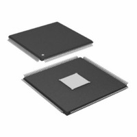
... COPLANARITY VIEW A VIEW A ROTATED 90° CCW Figure 22. 176-Lead Low Profile Quad Flat Package, Exposed Pad [LQFP_EP] ORDERING GUIDE Model Temperature Range 1 ADV3202ASWZ −40°C to +85°C ADV3203ASWZ 1 −40°C to +85° RoHS Compliant Part. 26.20 26.00 SQ 25.80 24.10 24. ...
Page 18
ADV3202/ADV3203 NOTES Rev Page ...
Page 19
NOTES Rev Page ADV3202/ADV3203 ...
Page 20
ADV3202/ADV3203 NOTES ©2008 Analog Devices, Inc. All rights reserved. Trademarks and registered trademarks are the property of their respective owners. D07526-0-10/08(0) Rev Page ...