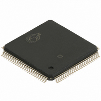
CY7C025AV-25AXC Cypress Semiconductor Corp, CY7C025AV-25AXC Datasheet

CY7C025AV-25AXC
Specifications of CY7C025AV-25AXC
CY7C025AV-25AXC
Available stocks
Related parts for CY7C025AV-25AXC
CY7C025AV-25AXC Summary of contents
Page 1
... A –A for 8K devices BUSY is an output in master mode and an input in slave mode. Cypress Semiconductor Corporation Document #: 38-06052 Rev. *M CY7C024AV/024BV/025AV/026AV 3.3V 4K/8K/16K x 16/18 Dual-Port Fully asynchronous operation ■ Automatic power down ■ Expandable data bus to 32 bits, 36 bits or more using Master ■ ...
Page 2
... IO 6 11L IO 12L 7 IO 13L 8 GND 14L IO 11 15L CY7C024AV/024BV (4K × 16 GND Notes the CY7C025AV. 12L the CY7C025AV. 12R Document #: 38-06052 Rev. *M CY7C024AV/024BV/025AV/026AV Figure 1. 100-Pin TQFP (Top View CY7C025AV (8K × 16 CY7C0241AV/0251AV/036AV INT 65 L BUSY 64 L GND 63 M/S 62 BUSY 61 R INT Page ...
Page 3
Pin Configurations (continued) 100 17L IO 5 11L IO 6 12L IO 13L 7 IO 14L 8 GND 15L IO 11 16L GND ...
Page 4
Pin Configurations (continued) 100 17L IO 5 11L IO 6 12L IO 13L 7 IO 14L 8 GND 15L IO 11 16L GND ...
Page 5
... CE pins. Data is available t asserted. If the user wants to access a semaphore flag, then the SEM pin and OE must be asserted. Interrupts The upper two memory locations are for message passing. The highest memory CY7C024AV/024BV/41AV/1FFF for the CY7C025AV/51AV, for 8K devices; A –A for 16K –IO for x18 devices) ...
Page 6
... CY7C026AV/36AV) is the mailbox for the right port and the second highest memory location (FFE for the CY7C024AV/024BV/41AV/1FFE for the CY7C025AV/51AV, 3FFE for the CY7C026AV/36AV) is the mailbox for the left port. When one port writes to the other port’s mailbox, an interrupt is generated to the owner ...
Page 7
Table 1. Non-Contending Read/Write Inputs CE R ...
Page 8
Maximum Ratings [14] Exceeding maximum ratings may shorten the useful life of the device. User guidelines are not tested. Storage Temperature ................................. –65°C to +150°C Ambient Temperature with Power Applied ............................................ –55°C to +125°C Supply Voltage to Ground Potential............... –0.5V ...
Page 9
R1 = 590 OUTPUT 435 (a) Normal Load (Load 1) 3.0V GND Switching Characteristics [20] Over the Operating Range Parameter Read Cycle t Read Cycle Time RC t Address to Data Valid AA ...
Page 10
Switching Characteristics [20] Over the Operating Range (continued) Parameter t Write Pulse Width PWE t Data Setup to Write End SD t Data Hold From Write End HD [23, 24] t R/W LOW to High Z HZWE [23, 24] t ...
Page 11
Switching Waveforms Figure 5. Read Cycle No. 1 (Either Port Address Access) ADDRESS OHA DATA OUT PREVIOUS DATA VALID Figure 6. Read Cycle No. 2 (Either Port CE/OE Access) CE and DATA OUT ...
Page 12
Switching Waveforms (continued) Figure 8. Write Cycle No. 1: R/W Controlled Timing ADDRESS OE [38, 39 R/W NOTE 41 DATA OUT DATA IN Figure 9. Write Cycle No Controlled Timing ADDRESS [38, 39 ...
Page 13
Switching Waveforms (continued) Figure 10. Semaphore Read After Write Timing, Either Side A –A VALID ADRESS SEM R/W OE Figure 11. Timing Diagram of Semaphore Contention A – R/W L ...
Page 14
Switching Waveforms (continued) Figure 12. Timing Diagram of Read with BUSY (M/S=HIGH) ADDRESS R R/W R DATA ADDRESS L BUSY L DATA OUTL Figure 13. Write Timing with Busy Input (M/S=LOW) R/W BUSY Note 47. CE ...
Page 15
Switching Waveforms (continued) Figure 14. Busy Timing Diagram No.1 (CE Arbitration) CE Valid First L ADDRESS L BUSY R CE Valid First: R ADDRESS L BUSY L Figure 15. Busy Timing Diagram ...
Page 16
Switching Waveforms (continued) Left Side Sets INT : R ADDRESS WRITE 1FFF (OR 1/3FFF R/W L INT R [50] t INS Right Side Clears INT : R ADDRESS R INT R ...
Page 17
... Asynchronous Dual-Port SRAM Speed (ns) Ordering Code 15 CY7C024BV-15AXI 20 CY7C024AV-20AXC CY7C024AV-20AXI 25 CY7C024AV-25AXC CY7C024AV-25AXI 8K x16 3.3V Asynchronous Dual-Port SRAM Speed (ns) Ordering Code 20 CY7C025AV-20AXC 25 CY7C025AV-25AXC CY7C025AV-25AXI 16K x16 3.3V Asynchronous Dual-Port SRAM Speed (ns) Ordering Code 20 CY7C026AV-20AXC 25 CY7C026AV-25AC CY7C026AV-25AXC CY7C026AV-25AI CY7C026AV-25AXI Ordering Code Definitions ...
Page 18
Package Diagram Figure 17. 100-Pin Pb-Free Thin Plastic Quad Flat Pack (TQFP) A100 Document #: 38-06052 Rev. *M CY7C024AV/024BV/025AV/026AV CY7C0241AV/0251AV/036AV 51-85048 *E Page [+] Feedback ...
Page 19
... Updated note number 33 on page 12 from “R/W must be HIGH during all address transitions” to “R must be HIGH during all address transitions” 12/17/08 Added CY7C024BV part 03/19/10 Removed inactive parts from ordering information table Updated package diagram Ordering Code Definitions. Part CY7C025AV-25AC from Ordering Information table. CY7C0241AV/0251AV/036AV Page [+] Feedback ...
Page 20
... Cypress against all charges. Any Source Code (software and/or firmware) is owned by Cypress Semiconductor Corporation (Cypress) and is protected by and subject to worldwide patent protection (United States and foreign), United States copyright laws and international treaty provisions. Cypress hereby grants to licensee a personal, non-exclusive, non-transferable license to copy, use, modify, create derivative works of, and compile the Cypress Source Code and derivative works for the sole purpose of creating custom software and or firmware in support of licensee product to be used only in conjunction with a Cypress integrated circuit as specified in the applicable agreement ...


