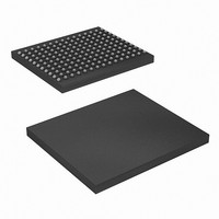
CY7C1315BV18-200BZI Cypress Semiconductor Corp, CY7C1315BV18-200BZI Datasheet - Page 15

CY7C1315BV18-200BZI
Manufacturer Part Number
CY7C1315BV18-200BZI
Description
SRAM (Static RAM)
Manufacturer
Cypress Semiconductor Corp
Datasheet
1.CY7C1313BV18-167BZC.pdf
(28 pages)
Specifications of CY7C1315BV18-200BZI
Format - Memory
RAM
Memory Type
SRAM - Synchronous, QDR II
Memory Size
18M (512K x 36)
Speed
200MHz
Interface
Parallel
Voltage - Supply
1.7 V ~ 1.9 V
Operating Temperature
-40°C ~ 85°C
Package / Case
165-LFBGA
Lead Free Status / RoHS Status
Contains lead / RoHS non-compliant
Available stocks
Company
Part Number
Manufacturer
Quantity
Price
Company:
Part Number:
CY7C1315BV18-200BZI
Manufacturer:
Cypress Semiconductor Corp
Quantity:
10 000
Document Number: 38-05620 Rev. *C
TAP Controller Block Diagram
TAP Electrical Characteristics
TAP AC Switching Characteristics
V
V
V
V
V
V
I
t
t
t
t
Set-up Times
t
t
t
Hold Times
t
t
Notes:
12. These characteristic pertain to the TAP inputs (TMS, TCK, TDI and TDO). Parallel load levels are specified in the Electrical Characteristics table.
13. t
14. Test conditions are specified using the load in TAP AC test conditions. t
15. Overshoot: V
16. All Voltage referenced to Ground.
X
TCYC
TF
TH
TL
TMSS
TDIS
CS
TMSH
TDIH
TDI
OH1
OH2
OL1
OL2
IH
IL
Parameter
Parameter
CS
and t
TCK
TMS
CH
refer to the set-up and hold time requirements of latching data from the boundary scan register.
IH
(AC) < V
Output HIGH Voltage
Output HIGH Voltage
Output LOW Voltage
Output LOW Voltage
Input HIGH Voltage
Input LOW Voltage
Input and Output Load Current
TCK Clock Cycle Time
TCK Clock Frequency
TCK Clock HIGH
TCK Clock LOW
TMS Set-up to TCK Clock Rise
TDI Set-up to TCK Clock Rise
Capture Set-up to TCK Rise
TMS Hold after TCK Clock Rise
TDI Hold after Clock Rise
Selection
Circuitry
DDQ
+ 0.85V (Pulse width less than t
Description
Over the Operating Range
106
31
Over the Operating Range
Boundary Scan Register
Description
30
.
Identification Register
Instruction Register
CYC
/2), Undershoot: V
29
.
I
I
I
I
GND ≤ V
TAP Controller
OH
OH
OL
OL
R
.
.
/t
F
= 2.0 mA
= 100 µA
= −2.0 mA
= −100 µA
Test Conditions
= 1 ns.
.
.
[12, 15, 16]
I
IL
≤ V
(AC) >
Bypass Register
2
2
2
DD
[13, 14]
−
1
1
1
1.5V (Pulse width less than t
0
0
0
0
0.65V
Min.
–0.3
1.4
1.6
–5
DD
Selection
Circuitry
Min.
50
20
20
CYC
5
5
5
5
5
CY7C1313BV18
CY7C1315BV18
CY7C1311BV18
CY7C1911BV18
/2).
V
0.35V
DD
Max.
Max.
0.4
0.2
20
5
+ 0.3
DD
Page 15 of 28
TDO
MHz
Unit
ns
ns
ns
ns
ns
ns
ns
ns
Unit
µA
V
V
V
V
V
V
[+] Feedback


