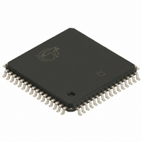
CY7C4245-15ASXC Cypress Semiconductor Corp, CY7C4245-15ASXC Datasheet

CY7C4245-15ASXC
Specifications of CY7C4245-15ASXC
Available stocks
Related parts for CY7C4245-15ASXC
CY7C4245-15ASXC Summary of contents
Page 1
... High speed 100 MHz operation (10 ns read/write cycle time) ■ Low power ( mA) CC ■ Fully asynchronous and simultaneous read and write operation ■ Empty, Full, Half Full, and Programmable Almost Empty/Almost Full status flags ■ ...
Page 2
... D 35 GND 2728 2930 CY7C4425/4205/4215 CY7C4225/4235/4245 FLAG PROGRAM REGISTER FF EF FLAG PAE LOGIC PAF SMODE READ POINTER READ CONTROL RCLK REN Figure 2. PLCC (Top View /SMODE GND CY7C4425 CY7C4205 CY7C4215 CY7C4225 CY7C4235 51 GND Q 50 CY7C4245 GND 3132 3940 4142 43 Page [+] Feedback ...
Page 3
... Cascaded – Connected to RXO of previous device. Not Cascaded – Tied to V CY7C4425/4205/4215 CY7C4225/4235/4245 -15 -25 - CY7C4235 CY7C4245 64-pin TQFP 64-pin TQFP ( 10) ( 10) 68-pin PLCC 68-pin PLCC (10 x 10) (10 x 10) /SMODE is tied /SMODE is tied standard mode of width expansion Retransmit function is also Page ...
Page 4
Pin Definitions (continued) Signal Name Description IO RXO Read Expansion O Output RS Reset I OE Output Enable I V /SMODE Synchronous I CC Almost Empty/ Almost Full Flags Architecture The CY7C42X5 consists of an array ...
Page 5
... Note Empty Offset (Default Values: CY7C4425 CY7C4205 n = 31, CY7C4215 n = 63, CY7C4225/CY7C4235/CY7C4245 n = 127 Full Offset (Default Values: CY7C4425 CY7C4205 n = 31, CY7C4215 n = 63, CY7C4225/CY7C4235/CY7C4245 n = 127). Document Number: 001-45652 Rev. *A that the FIFO is either Almost Full or Almost Empty. See for a description of programmable flags. ...
Page 6
Width Expansion Configuration The CY7C42X5 can be expanded in width to provide word widths greater than 18 in increments of 18. During width expansion mode all control line inputs are common and all flags are Figure 3. Block Diagram of ...
Page 7
Figure 4. Block Diagram of Synchronous FIFO Memory with Programmable Flags used in Depth Expansion Configuration FIRSTLOAD (FL) DATAIN (D) FIRSTLOAD (FL) WRITECLOCK (WCLK) WRITE ENABLE (WEN) RESET(RS) LOAD (LD) FF PAF FIRSTLOAD (FL) Document Number: 001-45652 Rev. *A WXO ...
Page 8
Maximum Ratings (Above which the useful life may be impaired. For user guidelines, not tested.) Storage Temperature ....................................−65 Ambient Temperature with Power Applied.................................................−55 Supply Voltage to Ground Potential .................−0.5V to +7.0V DC Voltage Applied to Outputs in High-Z State ...
Page 9
OUTPUT C L INCLUDING JIG AND SCOPE Equivalent to: THÉVENIN EQUIVALENT Rth = 410Ω OUTPUT Switching Characteristics Over the Operating Range Parameter Description t Clock Cycle Frequency S t Data Access Time A t Clock Cycle Time CLK t ...
Page 10
Switching Characteristics Over the Operating Range (continued) Parameter Description t Clock to Half-Full Flag HF t Clock to Expansion Out XO t Expansion in Pulse Width XI t Expansion in Set-up Time XIS t Skew Time between Read Clock and ...
Page 11
Switching Waveforms (continued) t RCLK t t ENS ENH REN EF Q – OLZ OE WCLK WEN RS REN, WEN, LD EF,PAE FF,PAF – Notes: 19 the minimum time between a ...
Page 12
Switching Waveforms (continued) Figure 9. First Data Word Latency after Reset with Simultaneous Read and Write WCLK –D D (FIRSTVALID WRITE ENS WEN t SKEW2 RCLK EF REN Q – ...
Page 13
Switching Waveforms (continued) NO WRITE WCLK t [18] SKEW1 D – WFF FF WEN RCLK t ENH t ENS REN LOW –q DATA IN OUTPUT REGISTER CLKH WCLK WEN HALF ...
Page 14
Switching Waveforms (continued) Figure 13. Programmable Almost Empty Flag Timing t CLKH WCLK WEN [24] PAE RCLK REN Figure 14. Programmable Almost Empty Flag Timing (applies only in SMODE (SMODE is LOW) t CLKH WCLK WEN PAE t SKEW3 RCLK ...
Page 15
... PAF offset = m. Number of data words written into FIFO already = 64 − for the CY7C4425, 256 − for the CY7C4205, 512 − for the CY7C4215. 1024 − for the CY7C4225, 2048 − for the CY7C4235, and 4096 − for the CY7C4245. 29. PAF is offset = m. ...
Page 16
Switching Waveforms (continued) t CLK t CLKH WCLK t ENS LD t ENS WEN – CLK t CLKH RCLK t ENS LD t ENS REN Q – CLKH WCLK WXO t ...
Page 17
Switching Waveforms (continued) t CLKH RCLK RXO t ENS REN WXI WCLK RXI RCLK FL/RT REN/WEN EF/FF and/all async flags HF/PAE/PAF Notes: 36. Read from Last Physical Location. 37. Clocks are free running in this case. 38. The flags may ...
Page 18
NORMALIZED SUPPLY CURRENT vs. SUPPLY VOLTAGE 1.4 1.2 1.0 V =3. =25°C 0.8 A f=100 MHz 0 4.5 5.5 SUPPLY VOLTAGE (V) NORMALIZED t vs.SUPPLY A VOLTAGE 1.2 T =25°C A 1.1 1.0 0.9 0.8 4 ...
Page 19
... Synchronous FIFO Speed (ns) Ordering Code 10 CY7C4225-10AXI 15 CY7C4225-15AXC CY7C4225-15ASXC Synchronous FIFO Speed (ns) Ordering Code 10 CY7C4245-10AXI 15 CY7C4245-15AXC CY7C4245-15ASXC Ordering Code Definitions Document Number: 001-45652 Rev. *A Package Name 51-85046 64-Pin (14 x 14) Thin Quad Flatpack (Pb-Free) Package Name 51-85046 64-Pin (14 x 14) Thin Quad Flatpack (Pb-Free) ...
Page 20
Package Diagrams Figure 25. 64-Pin Thin Plastic Quad Flat Pack ( 1.4 mm), 51-85046 Document Number: 001-45652 Rev. *A CY7C4425/4205/4215 CY7C4225/4235/4245 51-85046 *D Page [+] Feedback ...
Page 21
Package Diagrams (continued) Figure 26. 64-Pin Thin Plastic Quad Flat Pack ( 1.4 mm), 51-85051 Figure 27. 68-Pin Plastic Leaded Chip Carrier, 51-85005 Document Number: 001-45652 Rev. *A CY7C4425/4205/4215 CY7C4225/4235/4245 51-85051 *B 51-85005 *B Page 21 of ...
Page 22
... Document History Page Document Title: CY7C4425/CY7C4205/CY7C4215/CY7C4225/CY7C4235/CY7C4245, 64/256/512/1K/2K/ Synchronous FIFOs Document Number: 001-45652 REV. ECN NO. Issue Date ** 2489087 See ECN *A 3094407 11/24/10 © Cypress Semiconductor Corporation, 2008-2010. The information contained herein is subject to change without notice. Cypress Semiconductor Corporation assumes no responsibility for the use of any circuitry other than circuitry embodied in a Cypress product ...


