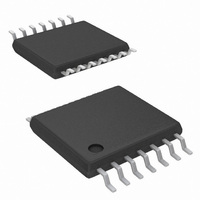
DG636EQ-T1-E3 Vishay, DG636EQ-T1-E3 Datasheet

DG636EQ-T1-E3
Specifications of DG636EQ-T1-E3
Available stocks
Related parts for DG636EQ-T1-E3
DG636EQ-T1-E3 Summary of contents
Page 1
... FEATURES • Ultra low charge injection (± 0.5 pC, typ. over the full analog signal range) • Leakage current < 0.5 nA max °C (for DG636EQ-T1-E3) • Low switch capacitance (C • Low R • Fully specified with single supply operation at 3.0 V, 5.0 V and dual supplies at ± 5.0 V • ...
Page 2
... mA Full On Switches DG636 All Switches Open D1 to S1A S2A D1 to S1B S2A D1 to S1A S2B D1 to S1B S2B Part Number DG636EQ-T1-E3 DG636EN-T1-E4 Limit 14 7 (V-) - 0.3 to (V mA, whichever occurs first 30 100 - 65 to 150 450 525 178 152 - 40 °C to 125 ° ° °C ...
Page 3
... Room pF MHz Room R Room pF MHz Room L L Room Room MHz Room Signal = kHz, RMS Room = 600 Vishay Siliconix - 40 °C to 125 ° ° ° Typ. Min. Max. Min 115 160 ± 0.01 - 0.1 0 0.5 ± 0. ...
Page 4
... DG636 Vishay Siliconix SPECIFICATIONS FOR DUAL SUPPLIES Parameter Symbol V Power Supplies Power Supply Current I+ Negative Supply Current I- I Ground Current GND SPECIFICATIONS FOR SINGLE SUPPLY V Parameter Symbol Analog Switch e V Analog Signal Range ANALOG R On-Resistance DS(on) R On-Resistance Match ON I Switch Off ...
Page 5
... Room D S Full Room V/3 V Full A0, A1 and ENABLE Full Under Test = 0 A0, A1 and ENABLE Full Under Test = 1 MHz Room Vishay Siliconix - 40 °C to 125 ° ° ° Typ. Min. Max. Min. Max. 0.009 2.5 6.4 11.3 0.001 0 0.001 - 0.5 - 0.5 ...
Page 6
... DG636 Vishay Siliconix SPECIFICATIONS FOR SINGLE SUPPLY V Parameter Symbol Dynamic Characteristics t Transition Time TRANS V t Enable Turn-On Time ON(EN) t Enable Turn-Off Time OFF(EN) Break-Before-Make- t BMM Time C Charge Injection Q e Off-Isolation OIRR e X Crosstalk TALK e Bandwidth BW Total Harmonic Distortion THD e C Source Off Capacitance ...
Page 7
... 120 100 400 350 + 25 ° °C 300 250 200 150 100 2 2 100 µA 10 µA 1 µ °C 100 100 Vishay Siliconix ° Analog Voltage (V) D On-Resistance vs. V (Dual Supply Voltage 5 125 ° ° ° ° 0 ...
Page 8
... DG636 Vishay Siliconix TYPICAL CHARACTERISTICS (25 °C, unless otherwise noted) 100 000 5 5 000 1000 100 I D(on Temperature (°C) Leakage Current vs. Temperature 10 LOSS ± 5 OIRR - 100 100K 1M 10M Frequency (Hz) Insertion Loss, Off-Isolation, Crosstalk vs. Frequency 100 3 5.0 V V± = ± 5.0 V 0.1 ...
Page 9
... S1A S2A V A0,A1 S2A or S2B S2A S2B 300 Ω Figure 1. Transition Time V+ V ENABLE V S1A 300 Ω Figure 2. Enable Switching Time V+ SxA - SxB V+ V A0, 300 Ω Figure 3. Break-Before-Make Vishay Siliconix t < < S1A S2A TRANS TRANS t < < S2A OFF t ON S1A or S2A < ...
Page 10
... Cross Talk = 20 log Figure 7. Crosstalk Vishay Siliconix maintains worldwide manufacturing capability. Products may be manufactured at one of several qualified locations. Reliability data for Silicon Technology and Package Reliability represent a composite of all qualified locations. For related documents such as package/tape drawings, part marking, and reliability data, see www.vishay.com/ppg?69901. ...
Page 11
... Vishay product could result in personal injury or death. Customers using or selling Vishay products not expressly indicated for use in such applications their own risk and agree to fully indemnify and hold Vishay and its distributors harmless from and against any and all claims, liabilities, expenses and damages arising or resulting in connection with such use or sale, including attorneys fees, even if such claim alleges that Vishay or its distributor was negligent regarding the design or manufacture of the part ...


