EVAL-ADF7021-NDBZ5 Analog Devices Inc, EVAL-ADF7021-NDBZ5 Datasheet - Page 22
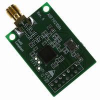
EVAL-ADF7021-NDBZ5
Manufacturer Part Number
EVAL-ADF7021-NDBZ5
Description
Matching Unpopulated
Manufacturer
Analog Devices Inc
Type
Transceiver, FSKr
Datasheet
1.ADF7021-NBCPZ-RL.pdf
(64 pages)
Specifications of EVAL-ADF7021-NDBZ5
Frequency
80MHz ~ 650MHz
Lead Free Status / RoHS Status
Lead free / RoHS Compliant
For Use With/related Products
ADF7021-N
Lead Free Status / Rohs Status
Supplier Unconfirmed


ADF7021-N
FREQUENCY SYNTHESIZER
REFERENCE INPUT
The on-board crystal oscillator circuitry (see Figure 32) can use
a quartz crystal as the PLL reference. Using a quartz crystal with
a frequency tolerance of ≤10 ppm for narrow-band applications
is recommended. It is possible to use a quartz crystal with >10 ppm
tolerance, but to comply with the absolute frequency error
specifications of narrow-band regulations (for example, ARIB
STD-T67 and ETSI EN 300 220), compensation for the
frequency error of the crystal is necessary.
The oscillator circuit is enabled by setting R1_DB12 high. It is
enabled by default on power-up and is disabled by bringing CE
low. Errors in the crystal can be corrected by using the automatic
frequency control feature or by adjusting the fractional-N value
(see the N Counter section).
Two parallel resonant capacitors are required for oscillation at
the correct frequency. Their values are dependent on the crystal
specification. They should be chosen to make sure that the
series value of capacitance added to the PCB track capacitance
adds up to the specified load capacitance of the crystal, usually
12 pF to 20 pF. Track capacitance values vary from 2 pF to 5 pF,
depending on board layout. When possible, choose capacitors
that have a very low temperature coefficient to ensure stable
frequency operation over all conditions.
Using a TCXO Reference
A single-ended reference (TCXO, VCXO, or OCXO) can also be
used with the ADF7021-N. This is recommended for applications
having absolute frequency accuracy requirements of <10 ppm, such
as applications requiring compliance with ARIB STD-T67 or
ETSI EN 300 220. The following are two options for interfacing
the ADF7021-N to an external reference oscillator.
•
•
Programmable Crystal Bias Current
Bias current in the oscillator circuit can be configured between 20
μA and 35 μA by writing to the XTAL_BIAS bits (R1_DB [13:14]).
Increasing the bias current allows the crystal oscillator to power
up faster.
An oscillator with CMOS output levels can be applied to
OSC2. The internal oscillator circuit should be disabled by
setting R1_DB12 low.
An oscillator with 0.8 V p-p levels can be ac-coupled through
a 22 pF capacitor into OSC1. The internal oscillator circuit
should be enabled by setting R1_DB12 high.
Figure 32. Oscillator Circuit on the ADF7021-N
OSC1
CP2
CP1
OSC2
Rev. 0 | Page 22 of 64
CLKOUT Divider and Buffer
The CLKOUT circuit takes the reference clock signal from the
oscillator section, shown in Figure 32, and supplies a divided-
down, 50:50 mark-space signal to the CLKOUT pin. The CLKOUT
signal is inverted with respect to the reference clock. An even
divide from 2 to 30 is available. This divide number is set in
R1_DB[7:10]. On power-up, the CLKOUT defaults to divide-by-8.
To disable CLKOUT, set the divide number to 0. The output
buffer can drive up to a 20 pF load with a 10% rise time at
4.8 MHz. Faster edges can result in some spurious feedthrough
to the output. A series resistor (1 kΩ) can be used to slow the
clock edges to reduce these spurs at the CLKOUT frequency.
R Counter
The 3-bit R counter divides the reference input frequency by an
integer between 1 and 7. The divided-down signal is presented
as the reference clock to the phase frequency detector (PFD). The
divide ratio is set in R1_DB[4:6]. Maximizing the PFD frequency
reduces the N value. This reduces the noise multiplied at a rate of
20 log(N) to the output and reduces occurrences of spurious
components.
Register 1 defaults to R = 1 on power-up.
Loop Filter
The loop filter integrates the current pulses from the charge
pump to form a voltage that tunes the output of the VCO to the
desired frequency. It also attenuates spurious levels generated by
the PLL. A typical loop filter design is shown in Figure 34.
The loop should be designed so that the loop bandwidth (LBW)
is approximately 100 kHz. This provides a good compromise
between in-band phase noise and out-of-band spurious rejection.
Widening the LBW excessively reduces the time spent jumping
between frequencies, but it can cause insufficient spurious attenua-
tion. Narrow-loop bandwidths can result in the loop taking long
periods to attain lock and can also result in a higher level of power
falling into the adjacent channel. The loop filter design on the
PFD [Hz] = XTAL/R
OSC1
PUMP OUT
CHARGE
Figure 34. Typical Loop Filter Configuration
DIVIDER
1 TO 15
Figure 33. CLKOUT Stage
÷2
DV
DD
VCO
CLKOUT
CLKOUT
ENABLE BIT
Related parts for EVAL-ADF7021-NDBZ5
Image
Part Number
Description
Manufacturer
Datasheet
Request
R

Part Number:
Description:
±1.7g Dual-Axis IMEMS Accelerometer Evaluation Board
Manufacturer:
Analog Devices Inc
Datasheet:

Part Number:
Description:
Inertial Sensor Evaluation System
Manufacturer:
Analog Devices Inc
Datasheet:
Part Number:
Description:
Manufacturer:
Analog Devices Inc
Datasheet:
Part Number:
Description:
Manufacturer:
Analog Devices Inc
Datasheet:
Part Number:
Description:
Manufacturer:
Analog Devices Inc
Datasheet:
Part Number:
Description:
Manufacturer:
Analog Devices Inc
Datasheet:
Part Number:
Description:
Manufacturer:
Analog Devices Inc
Datasheet:
Part Number:
Description:
Manufacturer:
Analog Devices Inc
Datasheet:
Part Number:
Description:
Manufacturer:
Analog Devices Inc
Datasheet:
Part Number:
Description:
Manufacturer:
Analog Devices Inc
Datasheet:
Part Number:
Description:
Manufacturer:
Analog Devices Inc
Datasheet:
Part Number:
Description:
Manufacturer:
Analog Devices Inc
Datasheet:
Part Number:
Description:
Manufacturer:
Analog Devices Inc
Datasheet: