JM38510/10103BGA National Semiconductor, JM38510/10103BGA Datasheet - Page 7
JM38510/10103BGA
Manufacturer Part Number
JM38510/10103BGA
Description
FULL JAN QUAL (LM101AH)
Manufacturer
National Semiconductor
Type
General Purpose Amplifierr
Datasheet
1.JM3851010103BGA.pdf
(22 pages)
Specifications of JM38510/10103BGA
Rail/rail I/o Type
No
Number Of Elements
1
Unity Gain Bandwidth Product
1MHz
Common Mode Rejection Ratio
80dB
Input Offset Voltage
2mV
Input Bias Current
75nA
Single Supply Voltage (typ)
Not RequiredV
Dual Supply Voltage (typ)
±9/±12/±15/±18V
Power Dissipation
1.2W
Voltage Gain In Db
80dB
Power Supply Rejection Ratio
86.02dB
Power Supply Requirement
Dual
Shut Down Feature
No
Single Supply Voltage (min)
Not RequiredV
Single Supply Voltage (max)
Not RequiredV
Dual Supply Voltage (min)
±5V
Dual Supply Voltage (max)
±22V
Technology
Bipolar
Operating Temp Range
-55C to 125C
Operating Temperature Classification
Military
Mounting
Through Hole
Pin Count
8
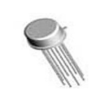
Package Type
TO-99
Lead Free Status / Rohs Status
Not Compliant
Available stocks
Company
Part Number
Manufacturer
Quantity
Price
Company:

Part Number:
JM38510/10103BGA
Manufacturer:
HITTITE
Quantity:
201


Symbol
V
±
IO
LM101A
DC Parameters:
The following conditions apply to all parameters, unless otherwise specified
V
Delta calculations performed on JAN S devices at group B, Subgroup 5 only.
Notes
Note 2: Absolute Maximum Ratings indicate limits beyond which damage to the device may occur. Operating ratings indicate conditions for which the device is
intended to be functional, but do no guarantee specific performance limits. For guaranteed specifications and test conditions, see the Electrical Characteristics. The
guaranteed specifications apply only for the test conditions listed. Some performance characteristics may degrade when the device is not operated under the listed
test conditions.
Note 3: For supply voltages less than
Note 4: The maximum power dissipation must be derated at elevated temperatures and is dictated by T
to ambient thermal resistance), and T
number given in the Absolute Maximum Ratings, whichever is lower.
Note 5: Human body model, 100 pF discharged through 1.5 kΩ.
Note 6: Calculated parameter
Note 7: Datalog reading of K = V/mV.
Note 8: Pin connections shown are for 8-pin packages.
I
IB
CC
=
±
20V, V
Parameter
Input Offset Voltage
Input Bias Current
CM
= 0V, R
JAN Electrical Characteristics
S
= 50Ω
A
±
(ambient temperature). The maximum allowable power dissipation at any temperature is P
15V, the absolute maximum input voltage is equal to the supply voltage.
Drift Values
Conditions
V
V
CM
CM
= 0V
= 0V, R
S
= 100KΩ
7
(Continued)
Jmax
Notes
(maximum junction temperature), θ
Min
-0.5
-7.5
Max
0.5
7.5
Dmax
= (T
Units
mV
Jmax
nA
JA
(package junction
− T
www.national.com
A
) / θ
groups
JA
Sub-
or the
1
1
Related parts for JM38510/10103BGA
Image
Part Number
Description
Manufacturer
Datasheet
Request
R

Part Number:
Description:
Manufacturer:
National Semiconductor
Datasheet:

Part Number:
Description:
Manufacturer:
National Semiconductor
Datasheet:
Part Number:
Description:
FULL JAN QUAL (LF411J)
Manufacturer:
National Semiconductor
Part Number:
Description:
Manufacturer:
National Semiconductor
Datasheet:
Part Number:
Description:
Manufacturer:
National Semiconductor
Datasheet:
Part Number:
Description:
Manufacturer:
National Semiconductor
Datasheet:


Part Number:
Description:
TUBE PACK, 300 MIL/N/A/JAN VERSION HA7-2600
Manufacturer:
Intersil Corporation
Part Number:
Description:
28 LD CERDIP/N/A/JAN VERSION HI1-0546
Manufacturer:
Intersil Corporation
Part Number:
Description:
TUBE PACK, 600 MIL/N/A/JAN VERSION HI1-0547
Manufacturer:
Intersil Corporation
Part Number:
Description:
MIL SPEC CMOS HEX NON-INVERTING BUFFER/CONVERTER
Manufacturer:
National Semiconductor
Part Number:
Description:
IC,Operational Amplifier,SINGLE,BIPOLAR,DIP,14PIN,CERAMIC
Manufacturer:
National Semiconductor
Datasheet:

Part Number:
Description:
JAN DG201AAP QUAD SPST CMOS ANALOG SWITCH
Manufacturer:
Intersil
Part Number:
Description:
QUAD 2 INPUT NAND GATE
Manufacturer:
National Semiconductor