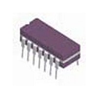
JM38510/11001BCA National Semiconductor, JM38510/11001BCA Datasheet - Page 10

JM38510/11001BCA
Manufacturer Part Number
JM38510/11001BCA
Description
FULL JAN QUAL (LM148J)
Manufacturer
National Semiconductor
Datasheet
1.JM3851011001BCA.pdf
(18 pages)
Specifications of JM38510/11001BCA
Rail/rail I/o Type
No
Number Of Elements
4
Unity Gain Bandwidth Product
1MHz
Common Mode Rejection Ratio
76dB
Input Offset Voltage
5@±5VmV
Input Bias Current
100nA
Single Supply Voltage (typ)
Not RequiredV
Dual Supply Voltage (typ)
±9/±12/±15/±18V
Power Dissipation
400mW
Voltage Gain In Db
80dB
Power Supply Rejection Ratio
80dB
Power Supply Requirement
Dual
Shut Down Feature
No
Single Supply Voltage (min)
Not RequiredV
Single Supply Voltage (max)
Not RequiredV
Dual Supply Voltage (min)
±5V
Dual Supply Voltage (max)
±22V
Technology
Bipolar
Operating Temp Range
-55C to 125C
Operating Temperature Classification
Military
Mounting
Through Hole
Pin Count
14
Package Type
CDIP
Number Of Channels
4
Voltage Gain Db
80 dB (Min)
Common Mode Rejection Ratio (min)
76 dB
Supply Current
3.6 mA at +/- 15 V
Maximum Power Dissipation
400 mW
Maximum Operating Temperature
+ 125 C
Package / Case
CDIP-14
Maximum Dual Supply Voltage
+/- 22 V
Minimum Operating Temperature
- 55 C
Lead Free Status / Rohs Status
Not Compliant
Available stocks
Company
Part Number
Manufacturer
Quantity
Price
Company:
Part Number:
JM38510/11001BCA
Manufacturer:
COPAL
Quantity:
5 510
Part Number:
JM38510/11001BCA
Manufacturer:
NS/国半
Quantity:
20 000
Company:
Part Number:
JM38510/11001BCA LM148J/883
Manufacturer:
XILINX
Quantity:
5
www.national.com
Application Hints
The LM148 series are quad low power LM741 op amps. In
the proliferation of quad op amps, these are the first to offer
the convenience of familiar, easy to use operating charac-
teristics of the LM741 op amp. In those applications where
LM741 op amps have been employed, the LM148 series op
amps can be employed directly with no change in circuit
performance.
The package pin-outs are such that the inverting input of
each amplifier is adjacent to its output. In addition, the
amplifier outputs are located in the corners of the package
which simplifies PC board layout and minimizes package
related capacitive coupling between amplifiers.
The input characteristics of these amplifiers allow differential
input voltages which can exceed the supply voltages. In
addition, if either of the input voltages is within the operating
common-mode range, the phase of the output remains cor-
rect. If the negative limit of the operating common-mode
range is exceeded at both inputs, the output voltage will be
positive. For input voltages which greatly exceed the maxi-
mum supply voltages, either differentially or common-mode,
resistors should be placed in series with the inputs to limit
the current.
Like the LM741, these amplifiers can easily drive a 100 pF
capacitive load throughout the entire dynamic output voltage
and current range. However, if very large capacitive loads
must be driven by a non-inverting unity gain amplifier, a
resistor should be placed between the output (and feedback
Typical Applications—LM148
f
R1 = 100k pot. C1 = 0.0047 µF, C2 = 0.01 µF, C3 = 0.1 µF, R2 = R6 = R7 = 1M,
R3 = 5.1k, R4 = 12Ω, R5 = 240Ω, Q = NS5102, D1 = 1N914, D2 = 3.6V avalanche
diode (ex. LM103), V
A simpler version with some distortion degradation at high frequencies can be made by using A1 as a simple inverting amplifier, and by putting back to back
zeners in the feedback loop of A3.
MAX
= 5 kHz, THD ≤ 0.03%
S
=
±
15V
One Decade Low Distortion Sinewave Generator
10
connection) and the capacitance to reduce the phase shift
resulting from the capacitive loading.
The output current of each amplifier in the package is limited.
Short circuits from an output to either ground or the power
supplies will not destroy the unit. However, if multiple output
shorts occur simultaneously, the time duration should be
short to prevent the unit from being destroyed as a result of
excessive power dissipation in the IC chip.
As with most amplifiers, care should be taken lead dress,
component placement and supply decoupling in order to
ensure stability. For example, resistors from the output to an
input should be placed with the body close to the input to
minimize “pickup” and maximize the frequency of the feed-
back pole which capacitance from the input to ground cre-
ates.
A feedback pole is created when the feedback around any
amplifier is resistive. The parallel resistance and capacitance
from the input of the device (usually the inverting input) to AC
ground set the frequency of the pole. In many instances the
frequency of this pole is much greater than the expected 3
dB frequency of the closed loop gain and consequently there
is negligible effect on stability margin. However, if the feed-
back pole is less than approximately six times the expected
3 dB frequency a lead capacitor should be placed from the
output to the input of the op amp. The value of the added
capacitor should be such that the RC time constant of this
capacitor and the resistance it parallels is greater than or
equal to the original feedback pole time constant.
20122708


